TPS65910, TPS65910A, TPS65910A3, TPS659101, TPS659102, TPS659103
TPS659104, TPS659105, TPS659106, TPS659107, TPS659108, TPS659109
www.ti.com
SWCS046N –MARCH 2010–REVISED APRIL 2012
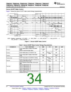
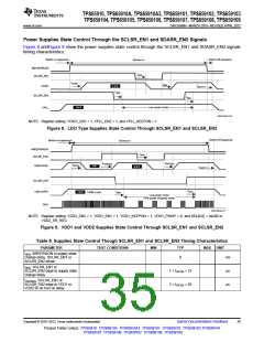
Power Supplies State Control Through the SCLSR_EN1 and SDASR_EN2 Signals
Figure 8 andFigure 9 show the power supplies state control through the SCLSR_EN1 and SDASR_EN2 signals
timing characteristics.
Switch-on sequence
Switch-off sequence
Device on
NRESPWRON
t
dEN
SCLSR_EN1
t
dVEN
t
dEN
VDIG1
t
dSOFF2
1.2 V
t
dEN
SCLSR_EN2
t
dEN
Low-power mode
1.8 V
VPLL
SWCS046-016
NOTE: Register setting: VDIG1_EN1 = 1, VPLL_EN2 = 1, and VPLL_KEEPON = 1
Figure 8. LDO Type Supplies State Control Through SCLSR_EN1 and SCLSR_EN2
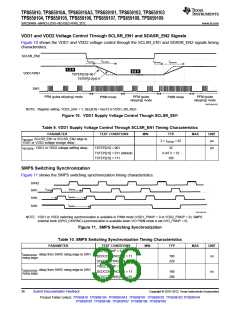
Switch-off sequence
Switch-on sequence
Device on
NRESPWRON
SCLSR_EN2
t
dEN
t
t
dVDDEN
dVDDEN
t
dOEN
VDD2/VFB2
0 V
3.3 V
t
dSOFF2
SCLSR_EN1
VDD1/VFB1
t
t
dEN
1.2 V
PWM mode
dEN
Low-power mode
PFM (pulse skipping) mode
SW1
SWCS046-017
NOTE: Register setting: VDD2_EN2 = 1, VDD1_EN1 = 1, VDD1_KEEPON = 1, VDD1_PSKIP = 0, and SEL[6:0] = hex00 in
VDD2_SR_REG
Figure 9. VDD1 and VDD2 Supplies State Control Through SCLSR_EN1 and SCLSR_EN2
Table 8. Supplies State Control Though SCLSR_EN1 and SCLSR_EN2 Timing Characteristics
PARAMETER
TEST CONDITIONS
MIN
TYP
MAX UNIT
tdEN: NREPSWON to supply state
change delay, SCLSR_EN1 or
SCLSR_EN2 driven
0
ms
µs
µs
tdEN: SCLSR_EN1 or
SCLSR_EN2 edge to supply state
change delay
1 × tCK32k = 31
3 × tCK32k = 63
tdVDDEN: SCLSR_EN1 or
SCLSR_EN2 edge to VDD1 or
VDD2 dc-dc turn on delay
Copyright © 2010–2012, Texas Instruments Incorporated
Submit Documentation Feedback
35
Product Folder Link(s): TPS65910 TPS65910A TPS65910A3 TPS659101 TPS659102 TPS659103 TPS659104
TPS659105 TPS659106 TPS659107 TPS659108 TPS659109

 TI [ TEXAS INSTRUMENTS ]