TPS65163
SLVSA28 –OCTOBER 2009
www.ti.com
DEVICE INFORMATION
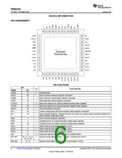
PIN ASSIGNMENT
SWB
CTRLN
FBN
1
2
36
35
34
33
32
31
30
29
28
27
26
25
SS
CRST
DLY
3
FBB
4
AGND
DISCH
VSENSE
VGH1
VGH2
RE
5
RST
VGL
6
Exposed
Thermal Die
7
FLK1
FLK2
FLK3
IN1
8
9
10
11
12
OUT1
OUT2
OUT3
IN2
IN3
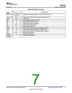
PIN FUNCTIONS
PIN
I/O
DESCRIPTION
NAME
AGND
BOOT
COMP
CRST
CTRLN
CTRLP
DISCH
DLY
NO.
33
48
37
35
2
P
I
Analog ground
Buck converter bootstrap capacitor connection
Boost converter compensation network connection.
Reset generator timing capacitor connection.
I
I
O
O
I
Base drive signal for an external transistor positive linear regulator
Base drive signal for an external transistor negative linear regulator
Panel discharging connection
40
32
34
38
I
Positive charge pump and boost converter delay capacitor connection
FB
I
Boost regulator feedback. Connect this pin to the center of a resistor divider connected between the
boost converter output and AGND.
FBB
4
3
I
I
Buck converter feedback connection
FBN
Feedback pin for an external transistor positive linear regulator
Feedback pin for an external transistor negative linear regulator
Flicker clock for level-shifter channels 1 and 4
FBP
39
7
I
FLK1
FLK2
FLK3
GD
I
8
1
I
Flicker clock for level-shifter channels 2 and 5
9
Flicker clock for level-shifter channels 3 and 6
41
O
I
Gate drive signal for the external MOSFET isolation switch
Inputs for level-shifter channels 1 through 7 (connected to VGH1)
IN1–IN7
10, 11, 12, 13,
14, 15, 16
IN8–IN9
17, 18
I
Inputs for level-shifter channels 8 and 9 (connected to VGH2)
6
Submit Documentation Feedback
Copyright © 2009, Texas Instruments Incorporated
Product Folder Link(s) :TPS65163

 TI [ TEXAS INSTRUMENTS ]