TPS65163
www.ti.com
SLVSA28 –OCTOBER 2009
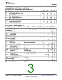
RECOMMENDED OPERATING CONDITIONS
over operating free-air temperature range (unless otherwise noted)
MIN
8.6
TYP
12
15
20
10
60
10
44
25
85
MAX
14.7
18.5
44
UNIT
V
VIN
VS
Supply voltage range
Boost converter output voltage range
Input capacitance
VIN + 1
10
V
CIN
L
µF
µH
µF
µH
µF
°C
°C
Boost converter inductance
Boost converter output capacitance
Buck converter inductance
Buck converter output capacitance
Operating ambient temperature
Operating junction temperature
6.8
15
COUT
L
40
100
15
6.8
COUT
TA
20
100
85
–40
–40
TJ
125
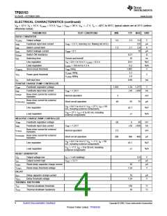
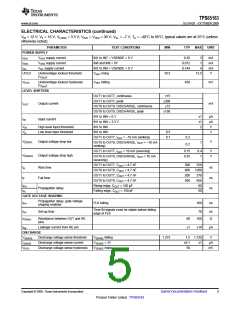
ELECTRICAL CHARACTERISTICS
VIN = 12 V; VS = 16 V; VLOGIC = 3.3 V; VGH1 = VGH2 = 30 V; VGL = –7 V; TA = –40°C to 85°C; typical values are at 25°C (unless
otherwise noted).
PARAMETER
TEST CONDITIONS
MIN
TYP
MAX
UNIT
POWER SUPPLY
IIN
Supply current
UVLO threshold
UVLO hysteresis
1
15
mA
V
UVLO
VHYS
7.8
8.2
8.5
V
INTERNAL OSCILLATOR
fSW Switching frequency
VOLTAGE REFERENCE
VREF Voltage reference
BOOST CONVERTER
600
750
900
kHz
V
1.24
VS
Output voltage
Measured after isolation switch
VFB = 1.24 V
VIN+1
1.228
18.5
V
V
VFB
IFB
Feedback regulation voltage
Feedback input bias current
Switch current limit
1.24 1.252
±0.01
3.5
±1
4.2
µA
A
ILIM
2.8
ILEAK
rDS(ON)
tSW
Switch leakage current
Switch ON resistance
Switching time
VSW = 15 V
10
µA
Ω
ISW = ILIM
0.15
10
0.25
Turnon and turnoff
ns
Line regulation
9.6 V < VIN < 14.4 V, IS = 750 mA
VS = 17 V, IS = 100 mA to 1.5 A
0.02
%/V
%/A
V
Load regulation
0.1
VOVP
ISS
Overvoltage threshold
Soft-start capacitor charge current
Short circuit threshold
1.03 × VFB
11
µA
mV
VFB(SC)
VFB rising
200
GATE DRIVE SIGNAL
VGD
ILK
Output low voltage
Leakage current
IGD = 500 µA (sinking)
VGD = 20 V
0.5
1
V
0.05
µA
Copyright © 2009, Texas Instruments Incorporated
Submit Documentation Feedback
3
Product Folder Link(s) :TPS65163

 TI [ TEXAS INSTRUMENTS ]