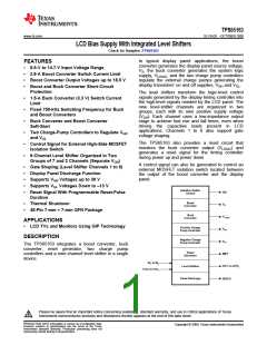
TPS65163
SLVSA28 –OCTOBER 2009
www.ti.com
This integrated circuit can be damaged by ESD. Texas Instruments recommends that all integrated circuits be handled with
appropriate precautions. Failure to observe proper handling and installation procedures can cause damage.
ESD damage can range from subtle performance degradation to complete device failure. Precision integrated circuits may be more
susceptible to damage because very small parametric changes could cause the device not to meet its published specifications.
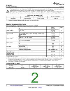
ORDERING INFORMATION(1)
TA
ORDERING
PACKAGE
PACKAGE MARKING
–40°C to 85°C
TPS65163RGZR
48-Pin 7x7 QFN
TPS65163
(1) The device is supplied taped and reeled, with 3000 (TBC) devices per reel.
ABSOLUTE MAXIMUM RATINGS
over operating free-air temperature range (unless otherwise noted)
(1)
VALUE
UNIT
VIN
–0.3 to 20
–0.3 to 45
0.3 to –15
Supply voltage(2)
Input voltage(2)
VGH1, VGH2
VGL
V
FBN, FBP, FBB, FB, DLY, CRST, SS, COMP, VL, FLK1–FLK3,
IN1–IN9, VSENSE
–0.3 to 7
V
V
RST
–0.3 to 7
–0.3 to 20
–0.3 to 45
–15 to 45
1
SWB, CTRLP, GD, SW, CTRLN
RE
Output voltage(2)
OUT1–OUT9, DISCHARGE
GD
Output current
ESD rating
mA
RE
100
Human-body model
Machine model
2000
V
V
200
Charged-device model
Continuous power dissipation
700
V
See Dissipation Table
W
Operating ambient
temperature range
–40 to 85
°C
Operating junction
temperature range
–40 to 150
–65 to 150
°C
°C
Storage temperature range
(1) Stresses beyond those listed under absolute maximum ratings may cause permanent damage to the device. These are stress ratings
only and functional operation of the device at these or any other conditions beyond those indicated under recommended operating
conditions is not implied. Exposure to absolute-maximum-rated conditions for extended periods may affect device reliability.
(2) With respect to the GND and AGND pins.
DISSIPATION RATINGS
T
A ≤ 25°C
TA = 70°C
POWER RATING
TA = 85°C
POWER RATING
PACKAGE
RθJA
POWER RATING
48-pin QFN
36 °C/W
2.78 W
1.53 W
1.11 W
2
Submit Documentation Feedback
Copyright © 2009, Texas Instruments Incorporated
Product Folder Link(s) :TPS65163

 TI [ TEXAS INSTRUMENTS ]