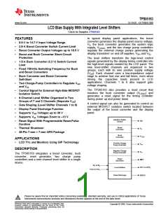
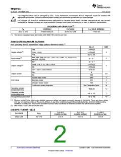
TPS65163
www.ti.com
SLVSA28 –OCTOBER 2009
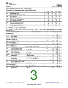
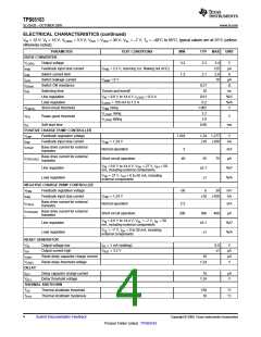
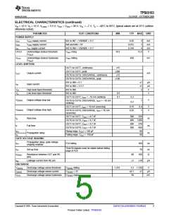
ELECTRICAL CHARACTERISTICS (continued)
VIN = 12 V; VS = 16 V; VLOGIC = 3.3 V; VGH1 = VGH2 = 30 V; VGL = –7 V; TA = –40°C to 85°C; typical values are at 25°C (unless
otherwise noted).
PARAMETER
POWER SUPPLY
TEST CONDITIONS
MIN
TYP
MAX
UNIT
IGH1
IGH2
IGL
VGH1 supply current
IN1 to IN7 = VSENSE = 0 V
0.35
0.012
0.144
3
1
mA
mA
mA
V
VGH2 supply current
IN8 and IN9 = 0V
IN1 to IN9 = VSENSE = 0 V
VGH1 rising
VGL supply current
4
UVLO
Undervoltage lockout threshold
10.5
13.5
(VGH1
Undervoltage lockout hysteresis
(VGH1
LEVEL SHIFTERS
)
VHYS
VGH1 falling
450
mV
)
OUT1 to OUT7, continuous
OUT1 to OUT7, peak
±15
±300
±15
IOUT
Output current
mA
OUT8 to OUT9, DISCGARGE, continuous
OUT8 to OUT9, DISCHARGE, peak
IN1 to IN9 = 0 V
±150
±1
±1
2
µA
µA
V
IIN
Input current
IN1 to IN9 = 3.3 V
VIH
VIL
High level input threshold
Low level input threshold
IN1 to IN9
IN1 to IN9
0.5
0.1
V
OUT1 to OUT7, IOUT = –10 mA (sinking)
0.3
0.2
VDROPL
Output voltage drop low
Output voltage drop high
V
OUT8 to OUT9, DISCHARGE, IOUT = –10 mA
(sinking)
1
OUT1 to OUT7, IOUT = 10 mA (sourcing)
0.15
0.35
0.4
1
V
V
VDROPH
OUT8 to OUT9, DISCHARGE, IOUT = 10 mA
(sourcing)
OUT1 to OUT7, COUT = 4.7 nF
OUT8 to OUT9, COUT = 4.7 nF
OUT1 to OUT7, COUT = 4.7 nF
OUT8 to OUT9, COUT = 4.7 nF
Rising edge, COUT = 150 pF
Falling edge, COUT = 150 pF
300
800
200
500
520
1200
370
850
60
tR
Rise time
ns
ns
ns
tF
Fall time
tPH
tPL
Propagation delay
60
GATE VOLTAGE SHAPING
Propagation delay, gate voltage
shaping enabled
tPH
FLK falling
100
ns
Time IN signals must be stable before falling
edge of FLK
tSU
Set-up time
70
ns
rDS(on)
Resistance between OUT and RE
pins
60
±1
100
Ω
Ilkg
Leakage current from RE pin
±10
µA
DISCHARGE
VSENSE
ISENSE
VHYS
Discharge voltage sense threshold
VSENSE falling
VSENSE = 2V
VSENSE rising
1.275
1.5 1.725
±0.1 ±1
50
V
Discharge voltage sense current
Discharge voltage sense hysteresis
µA
mV
Copyright © 2009, Texas Instruments Incorporated
Submit Documentation Feedback
5
Product Folder Link(s) :TPS65163

 TI [ TEXAS INSTRUMENTS ]