TPS65163
www.ti.com
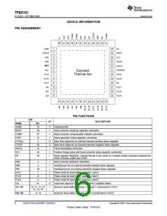
NAME
SLVSA28 –OCTOBER 2009
PIN FUNCTIONS (continued)
PIN
I/O
DESCRIPTION
NO.
OUT7–OUT1 21, 22, 23, 24,
25, 26, 27
O
Outputs for level-shifter channels 1 through 7 (connected to VGH1)
OUT9–OUT8
PGND
RE
19, 20
44, 45
28
O
P
O
O
I
Outputs for level-shifter channels 8 and 9 (connected to VGH2)
Power ground
Gate shaping slope resistor connection
Reset generator open-drain output
RST
5
SS
36
Soft-start timing-capacitor connection.
Boost converter switching node
SW
42, 43
1
O
O
P
P
P
P
I
SWB
Buck converter switch node
VGH1
VGH2
VGL
30
Positive supply voltage for level-shifter channels 1 through 7
Positive supply voltage for level-shifter channels 8 and 9
Negative supply voltage for level-shifter channels 1 through 9
Supply-voltage connection
29
6
VIN
46, 47
31
VSENSE
Discharge sense voltage
Exposed
P
Connect to the system GND
thermal die
Copyright © 2009, Texas Instruments Incorporated
Submit Documentation Feedback
7
Product Folder Link(s) :TPS65163

 TI [ TEXAS INSTRUMENTS ]