TPS61199
www.ti.com
SLVSAN3 –DECEMBER 2010
Output Capacitor
The output capacitor is mainly selected to meet the requirements for output ripple and loop stability of the whole
system. This ripple voltage is related to the capacitance of the capacitor and its equivalent series resistance
(ESR). Assuming a capacitor with zero ESR, the minimum capacitance needed for a given ripple can be
calculated by:
D
× I
MAX
OUT
OUT
V
=
rippleC
F
× C
SW
(7)
Where Vripplec is the peak to peak output ripple, and DMAX is the duty cycle of the boost converter. DMAX is equal
to approximately (VOUT_MAX - VIN_MIN) / VOUT_MAX in applications.
Care must be taken when evaluating a capacitor’s derating under dc bias. The DC bias can also significantly
reduce capacitance. Ceramic capacitors can loss as much as 50% of its capacitance at its rated voltage.
Therefore, leave the margin on the voltage rating to ensure adequate capacitance in the recommendation table.
The ESR impact on the output ripple must be considered as well if tantalum or electrolytic capacitors are used.
Assuming there is enough capacitance such that the ripple due to the capacitance can be ignored, the ESR
needed to limit the Vripple is:
V
= I
× ESR
rippleESR
LPeak
(8)
Ripple current flowing through a capacitor’s ESR causes power dissipation in the capacitor. This power
dissipation causes a temperature increase internal to the capacitor. Excessive temperature can seriously shorten
the expected life of a capacitor. Capacitors have ripple current ratings that are dependent on ambient
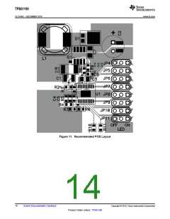
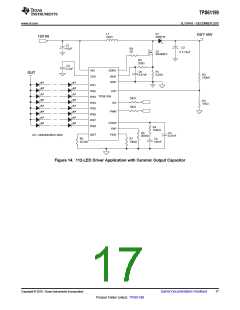
temperature and should not be exceeded. Therefore, three electrolytic capacitors (UPW2A330MPD6, Nichicon)
in parallel reduces the total ESR, shown as Figure 1.
In typical application, The output requires a capacitor in the range of 10µF to 100µF. The output capacitor affects
the small signal control loop stability of the boost converter. If the output capacitor is below the range, the boost
regulator may potentially become unstable.
Loop Consideration
The COMP pin on the TPS61199 is used for external compensation, allowing the loop response to be optimized
for each application. The COMP pin is the output of the internal transconductance amplifier. The external resistor
R4, along with ceramic capacitors C4 and C5, are connected to the COMP pin to provide poles and zero. The
poles and zero, along with the inherent pole and zero in a peak current mode control boost converter, determine
the closed loop frequency response. This is important to converter stability and transient response. For most of
the applications, the recommended value of 10kΩ for R4, 100nF for C4 and 470pF for C5 are sufficient. For
applications with different components or requirements, please refer to application note SLVA452 “Compensating
the Current Mode Boost Converter” for guidance on selecting different compensation components.
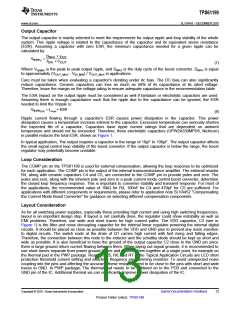
Layout Consideration
As for all switching power supplies, especially those providing high current and using high switching frequencies,
layout is an important design step. If layout is not carefully done, the regulator could show instability as well as
EMI problems. Therefore, use wide and short traces for high current paths. The VDD capacitor, C3 (see in
Figure 1) is the filter and noise decoupling capacitor for the internal linear regulator powering the internal digital
circuits. It should be placed as close as possible between the VDD and GND pins to prevent any noise insertion
to digital circuits. The switch node at the drain of Q1 carries high current with fast rising and falling edges.
Therefore, the connection between this node to the inductor and the schottky diode should be kept as short and
wide as possible. It is also beneficial to have the ground of the output capacitor C2 close to the GND pin since
there is large ground return current flowing between them. When laying out signal grounds, it is recommended to
use short traces separate from power ground traces and connect them together at a single point, for example on
the thermal pad in the PWP package. Resistors R5, R6, and R7 in the Typical Application Circuits are LED short
protection threshold current setting and switching frequency programming resistors. To avoid unexpected noise
coupling into the pins and affecting the accuracy, these resistors need to be close to the pins with short and wide
traces to GND. In PWP package, The thermal pad needs to be soldered on to the PCB and connected to the
GND pin of the IC. Additional thermal via can significantly improve power dissipation of the IC.
Copyright © 2010, Texas Instruments Incorporated
Submit Documentation Feedback
13
Product Folder Link(s): TPS61199

 TI [ TEXAS INSTRUMENTS ]