TPS61199
SLVSAN3 –DECEMBER 2010
www.ti.com
APPLICATION INFORMATION
Inductor Selection
The TPS61199 is designed to work with inductor values between 10µH to 47µH. Running the controller at higher
switching frequencies allows the use of smaller and/or lower profile inductors in the 10µH range. Running the
controller at slower switching frequencies requires the use of larger inductors, near 47µH, to maintain the same
inductor current ripple but may improve overall inefficiency due to smaller switching losses. Inductor values can
have ±20% tolerance with no current bias. When the inductor current approaches saturation level, its inductance
can decrease 20% to 35% from the 0A value depending on how the inductor vendor defines saturation. In a
boost regulator, the inductor peak current can be calculated with Equation 5 and Equation 6.
V
× I
I
PP
OUT
OUT
I
=
+
LPeak
V
× η
2
IN
(5)
1
DIL =
æ
ç
è
ö
´ FSW
÷
1
1
L ´
+
VOUT - V
V
IN ø
IN
(6)
Where:
VOUT = output voltage
IOUT = total LED current
VIN = input voltage
h = power conversion efficiency, use 85% for TPS61199 applications
L = inductor value
FSW = switching frequency
Select an inductor with a saturation current over the calculated peak current. To calculate the worst case inductor
peak current, use the minimum input voltage, maximum output voltage, and maximum total LED current. Select
an inductor with a saturation current at least 30% higher the calculated peak current to account for load
transients when dimming. Table 2 lists the recommended inductors
Table 3. Recommended Value for Inductor
L(µH)
22
DCR (mΩ)
48.8
ISAT (A)
5.6
SIZE (LxWxH mm)
12.5 x 12.5 x 8.0
12.5 x 12.5 x 7.5
12.8 x 12.8 x 6.8
MFR.
Sumida
TDK
CDRH127/HPNP-220M
SLF12575T- 220M
#B953AS-220M
22
26.3
4
22
46
3.6
TOKO
Schottky Diode
The TPS61199 demands a high-speed rectification for optimum efficiency. Ensure theat the diode's average and
peak current rating exceed the output LED current and inductor peak current. In addition, the diode's reverse
breakdown voltage must exceed the application output voltage. Therefore, the VISHAY SS5P9 is recommended.
Switch MOSFET And Gate Driver Resistor
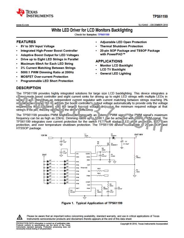
The TPS61199 demands a power N-MOSFET (See Q1 in Figure 1) as a switch. The voltage and current rating
of the MOSFET must be higher than the application output voltage and the inductor peak current. The
applications benefits from the addition of a resistor (See R8 in Figure 1) connected between the GDRV pin and
the gate of the switching MOSFET. With this resistor, the load regulation between LED dimming on and off
period and EMI are improved. A 3-Ω resistor value is recommended. The TPS61199 exhibits lower efficiency
when the resistor value is above 3Ω.
Current Sense Filtering
A small filter placed on the ISNS pin improves performance of the converter (See R9 and C6 in Figure 1). The
time constant of this filter should be approximately 100ns. The range of R9 should be from about 100Ω to 1kΩ
for best results. The C6 should be located as close as possible to the ISNS pin to provide noise immunity.
12
Submit Documentation Feedback
Copyright © 2010, Texas Instruments Incorporated
Product Folder Link(s): TPS61199

 TI [ TEXAS INSTRUMENTS ]