PDF
最近搜索
热门搜索
发布采购

| 型号: | TPS61196 |
| PDF下载: | 下载PDF文件 查看货源 |
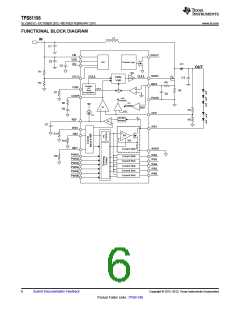
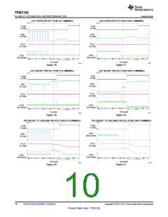
| 内容描述: | 6串400 mA的WLED驱动器,带有独立的PWM调光的每个字符串 [6-String 400-mA WLED Driver with Independent PWM Dimming for Each String] |
| 分类和应用: | 驱动器 |
| 文件页数/大小: | 30 页 / 1948 K |
| 品牌: |  TI [ TEXAS INSTRUMENTS ] TI [ TEXAS INSTRUMENTS ] |
专业IC领域供求交易平台:提供全面的IC Datasheet资料和资讯,Datasheet 1000万数据,IC品牌1000多家。