TPS61196
www.ti.com
SLVSBG1C –OCTOBER 2012–REVISED FEBRUARY 2013
DEVICE INFORMATION
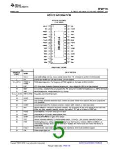
HTSSOP-28 (PWP)
(TOP VIEW)
UVLO
EN
1
28
27
26
25
24
23
22
21
20
19
18
17
16
15
VIN
2
FAULT
FSW
VDD
PWM1
PWM2
PWM3
PWM4
PWM5
PWM6
FBP
3
4
5
GDRV
ISNS
PGND
REF
6
7
8
9
COMP
OVP
ISET
10
11
12
13
14
IFBV
IFB1
AGND
IFB6
IFB2
IFB5
IFB3
IFB4
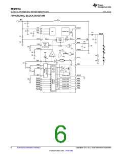
PIN FUNCTIONS
PIN
DESCRIPTION
NUMBER
(PWP)
NAME
1
2
UVLO
EN
Low input voltage lock out. Use a resister divider from VIN to this pin to set the UVLO threshold
Enable and disable pin. EN high=Enable, EN low=Disable
3,4,5,6,7,8
PWM1 to
PWM6
PWM signal input pins. The frequency of PWM signal is in the range of 90Hz to 22kHz
9
FBP
ISET
IFBV
LED cross-short protection threshold program pin. Use a resistor to GND to set the threshold
Connecting a resistor to the pin programs the IFB pin current level for full brightness (i.e., 100% dimming)
Minimum feedback voltage setting for LED strings
10
11
12,13,14,15,16, IFB1 to IFB6 Regulated current sink input pins
17
18
19
AGND
OVP
Analog ground
Over-voltage protection detection input. Connect a resistor divider from output to this pin to program the
OVP threshold.
20
21
COMP
REF
Loop compensation for the boost converter. Connect a RC network to make loop stable
Internal reference voltage for the boost converter. Use a capacitor at this pin to adjust the soft start time.
When two chips operate in parallel, connect the master's REF pin to the slave's COMP pin.
22
23
24
25
26
PGND
ISNS
GDRV
VDD
External MOSFET current sense ground input
External MOSFET current sense positive input
External switch MOSFET gate driver output
Internal regulator output for IC internal power supply. Connect a 1.0µF ceramic capacitor to this pin.
FSW
Switching frequency setting pin. Use a resistor to set the frequency between 100kHz to 800kHz. An
external input voltage above 3.5V or below 0.5V disables the internal clock and makes the device as
slave device
27
28
FAULT
VIN
Fault indicator. Open-drain output. Output high impedance when fault conditions happen
Power supply input pin
Copyright © 2012–2013, Texas Instruments Incorporated
Submit Documentation Feedback
5
Product Folder Links :TPS61196

 TI [ TEXAS INSTRUMENTS ]