TPS5430
www.ti.com
SLVS632–JANUARY 2006
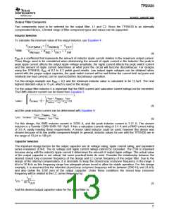
This equation assumes nominal on resistance for the high side FET and accounts for worst case variation of
operating frequency set point. Any design operating near the operational limits of the device should be
carefully checked to assure proper functionality.
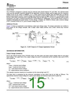
Internal Compensation Network
The design equations given in the example circuit can be used to generate circuits using the TPS5430. These
designs are based on certain assumptions and will tend to always select output capacitors within a limited range
of ESR values. If a different capacitor type is desired, it may be posssible to to fit one to the internal
compensation of the TPS5430. Equation 15 gives the nominal frequency response of the internal voltage-mode
type III compensation network:
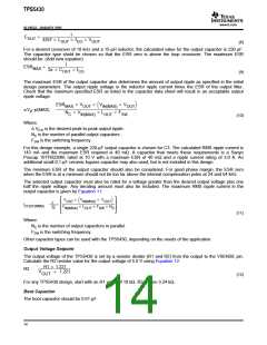
s
s
1 )
1 )
2p Fz1
2p Fz2
H(s)
s
s
s
s
ǒ Ǔ ǒ
Ǔ ǒ
1 )
Ǔ ǒ
Ǔ
1 )
1 )
2p Fp0
2p Fp1
2p Fp2
2p Fp3
(15)
Where
Fp0 = 2165 Hz, Fz1 = 2170 Hz, Fz2 = 2590 Hz
Fp1 = 24 kHz, Fp2 = 54 kHz, Fp3 = 440 kHz
Fp3 represents the non-ideal parasitics effect.
Using this information along with the desired output voltage, feed forward gain and output filter characteristics,the
closed loop transfer function can be derived.
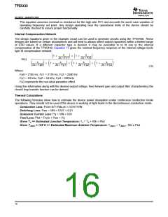
Thermal Calculations
The following formulas show how to estimate the device power dissipation under continuous conduction mode
operations. They should not be used if the device is working at light loads in the discontinuous conduction mode.
Conduction Loss: Pcon=Io2× Rds,on × VOUT/VIN
Switching Loss: Psw = VIN × IOUT × 0.01
Quiescent Current Loss: Pq = VIN × 0.01
Total Loss: Ptot = Pcon + Psw + Pq
Given TA => Estimated Junction Temperature: TJ = TA + Rth × Ptot
Given TJMAX = 125°C => Estimated Maximum Ambient Temperature: TAMAX = TJMAX– Rth x Ptot
16

 TI [ TEXAS INSTRUMENTS ]