TPS54232
www.ti.com ........................................................................................................................................................................................... SLVS876–NOVEMBER 2008
VREF = 0.8 V
With RZ known, CZ and CP can be calculated using Equation 26 and Equation 27:
1
CZ =
2´p ´ FZ1 ´ Rz
(26)
1
CP =
2´p ´ FP1 ´ Rz
(27)
For this design, a 22-µF output capacitor isused. For ceramic capacitors, the actual output capacitance is less
than the rated value when the capacitors have a dc bias voltage applied. This is the case in a dc/dc converter.
For this dsign, a 10 V capacitor is chosen to minimize this effect. The ESR is approximately .005 Ω.
Using Equation 19 and Equation 20, the output stage gain and phase loss are equivalent as:
Gain = 1.613 dB
and
PL = -92.3 degrees
For 60 degrees of phase margin, Equation 21 requires 62.33 degrees of phase boost.
Equation 22, Equation 23, and Equation 24 are used to find the zero and pole frequencies of:
FZ1 = 12.3 k Hz
And
FP1 = 203 kHz
RZ, CZ, and CP are calculated using Equation 25, Equation 26, and Equation 27:
2 ´ p ´ 50000 ´ 2.5 ´ 22 ´ 10-6 ´ 8.696 ´ 106 ´0.79
Rz =
Cz =
Cp =
= 17.7 kW
10 ´ 800 ´ 0.8
(28)
(29)
(30)
1
= 730 pF
2 ´ p ´ 12300 ´ 17700
1
= 44 pF
2 ´ p ´ 203000 ´ 17700
Using standard values for R3, C6, and C7 in the application schematic of Figure 13:
R3 = 17.4 kΩ
C6 = 680 pF
C7 = 47 pF
BOOTSTRAP CAPACITOR
Every TPS54232 design requires a bootstrap capacitor, C4. The bootstrap capacitor must be 0.1 µF. The
bootstrap capacitor is located between the PH pins and BOOT pin. The bootstrap capacitor should be a
high-quality ceramic type with X7R or X5R grade dielectric for temperature stability.
CATCH DIODE
The TPS54232 is designed to operate using an external catch diode between PH and GND. The selected diode
must meet the absolute maximum ratings for the application: Reverse voltage must be higher than the maximum
voltage at the PH pin, which is VINMAX + 0.5 V. Peak current must be greater than IOUTMAX plus on half the
peak to peak inductor current. Forward voltage drop should be small for higher efficiencies. It is important to note
that the catch diode conduction time is typically longer than the high-side FET on time, so attention paid to diode
parameters can make a marked improvement in overall efficiency. Additionally, check that the device chosen is
capable of dissipating the power losses. For this design, a Diodes, Inc. B220A is chosen, with a reverse voltage
of 20 V, forward current of 2A, and a forward voltage drop of 0.5 V.
Copyright © 2008, Texas Instruments Incorporated
Submit Documentation Feedback
15
Product Folder Link(s): TPS54232

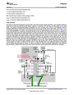
 TI [ TEXAS INSTRUMENTS ]