TPS54232
SLVS876–NOVEMBER 2008 ........................................................................................................................................................................................... www.ti.com
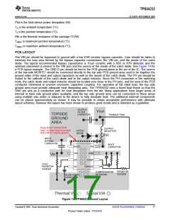
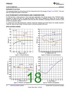
Estimated Circuit Area
The estimated printed circuit board area for the components used in the design of Figure 13 is 0.44 in2. This area
does not include test points or connectors.
ELECTROMAGNETIC INTERFERENCE (EMI) CONSIDERATIONS
As EMI becomes a rising concern in more and more applications, the internal design of the TPS54232 takes
measures to reduce the EMI. The high-side MOSFET gate drive is designed to reduce the PH pin voltage
ringing. The internal IC rails are isolated to decrease the noise sensitivity. A package bond wire scheme is used
to lower the parasitics effects.
To achieve the best EMI performance, external component selection and board layout are equally important.
Follow the Step by Step Design Procedure above to prevent potential EMI issues.
APPLICATION CURVES
100
100
95
90
85
80
V
= 3.3 V
O
95
V = 8 V
I
V = 5 V
I
90
V = 12 V
85
I
V = 12 V
I
80
75
70
75
70
65
60
V = 15 V
I
V = 15 V
I
65
60
55
50
0
0.25 0.5 0.75
1
1.25 1.5 1.75
2
0
0.02 0.04 0.06 0.08 0.1 0.12 0.14 0.16 0.18 0.2
- Output Current - mA
I
I
- Output Current - A
O
O
Figure 15. TPS54232 Efficiency
Figure 16. TPS54232 Low Current Efficiency
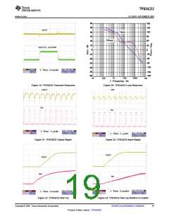
0.1
0.08
0.06
0.04
0.02
0
0.025
0.02
0.015
0.01
V = 15 V
I
V = 5 V
I
I
= 1 A
O
0.005
0
-0.005
-0.01
-0.015
-0.02
-0.04
-0.06
V = 12 V
I
-0.02
-0.08
-0.1
-0.025
0
0.2 0.4 0.6 0.8
I
1
- Output Current - A
1.2 1.4 1.6 1.8
2
5
6
7
8
9
V - Input Voltage - V
10 11 12 13 14 15
O
I
Figure 17. TPS54232 Load Regulation
Figure 18. TPS54232 Line Regulation
18
Submit Documentation Feedback
Copyright © 2008, Texas Instruments Incorporated
Product Folder Link(s): TPS54232

 TI [ TEXAS INSTRUMENTS ]