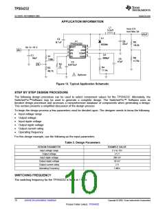
TPS54232
SLVS876–NOVEMBER 2008 ........................................................................................................................................................................................... www.ti.com
maximum closed loop crossover frequency be not greater than 75 kHz. Next, the required gain and phase boost
of the crossover network needs to be calculated. By definition, the gain of the compensation network must be the
inverse of the gain of the modulator and output filter. For this design example, where the ESR zero is much
higher than the closed loop crossover frequency, the gain of the modulator and output filter can be approximated
by Equation 19:
Gain = - 20 log 2 ´ p ´ R
(
´FCO ´CO - 2dB
)
SENSE
(19)
Where:
RSENSE = 1Ω/10
FCO = Closed-loop crossover frequency
CO = Output capacitance
The phase loss is given by Equation 20:
PL = a tan 2 ´ p ´ FCO ´RESR ´ CO - a tan 2 ´ p ´ FCO ´RO ´ CO -10deg
(
(
)
)
(20)
Where:
RESR = Equivalent series resistance of the output capacitor
RO = VO/IO
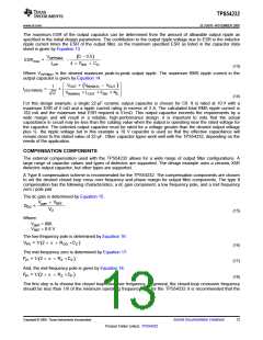
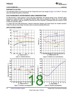
The measured overall loop response for the circuit is given in Figure 20. Note that the actual closed loop
crossover frequency is higher than intended at about 25 kHz. This is primarily due to variation in the actual
values of the output filter components and tolerance variation of the internal feed-forward gain circuitry. Overall
the design has greater than 60 degrees of phase margin and will be completely stable over all combinations of
line and load variability.
Now that the phase loss is known the required amount of phase boost to meet the phase margin requirement
can be determined. The required phase boost is given by Equation 21:
PB = PM - 90deg -PL
)
(
(21)
Where PM = the desired phase margin.
A zero / pole pair of the compensation network will be placed symmetrically around the intended closed loop
frequency to provide maximum phase boost at the crossover point. The amount of separation can be determined
by Equation 22 and the resultant zero and pole frequencies are given by Equation 23 and Equation 24
PB
æ
ç
è
ö
÷
ø
k = tan
+ 45deg
2
(22)
FCO
k
FZ1 =
(23)
(24)
FP1 = FCO ´k
The low-frequency pole is set so that the gain at the crossover frequency is equal to the inverse of the gain of the
modulator and output filter. Due to the relationships established by the pole and zero relationships, the value of
RZ can be derived directly by Equation 25 :
2 × p × FCO × VO × CO × ROA × 0.79
RZ
=
GM
× Vggm × VREF
ICOMP
(25)
Where:
VO = Output voltage
CO = Output capacitance
FCO = Desired crossover frequency
ROA = 8.696 MΩ
GMCOMP = 10 A/V
Vggm = 800
14
Submit Documentation Feedback
Copyright © 2008, Texas Instruments Incorporated
Product Folder Link(s): TPS54232

 TI [ TEXAS INSTRUMENTS ]