TPS54232
SLVS876–NOVEMBER 2008 ........................................................................................................................................................................................... www.ti.com
OUTPUT VOLTAGE LIMITATIONS
Due to the internal design of the TPS54232, there are both upper and lower output voltage limits for any given
input voltage. The upper limit of the output voltage set point is constrained by the maximum duty cycle of 90%
and is given by Equation 31:
VOmax = 0.90 ×
V
(
(
- IO max × RDSon max + V
)
-
I
(
× RL - VD
)
)
IN min
D
O max
(31)
Where:
VIN min = Minimum input voltage
IO max = Maximum load current
VD = Catch diode forward voltage
RL = Output inductor series resistance
The equation assumes maximum on resistance for the internal high-side FET.
The lower limit is constrained by the minimum controllable on time which may be as high as 135 ns. The
approximate minimum output voltage for a given input voltage and minimum load current is given by Equation 32:
VOmin = 0.162 ´
V
(
(
- IOmin ´ Rin + V
)
-
I
(
´ RL - VD
)
)
IN max
D
O min
(32)
Where:
VIN max = Maximum input voltage
IO min = Minimum load current
VD = Catch diode forward voltage
RL = Output inductor series resistance
This equation assumes nominal on-resistance for the high-side FET and accounts for worst case variation of
operating frequency set point. Any design operating near the operational limits of the device should be carefully
checked to assure proper functionality.
POWER DISSIPATION ESTIMATE
The following formulas show how to estimate the device power dissipation under continuous conduction mode
operations. They should not be used if the device is working in the discontinuous conduction mode (DCM) or
pulse skipping Eco-modeTM
.
The device power dissipation includes:
1) Conduction loss: Pcon = IOUT2 x Rds(on) x VOUT/VIN
2) Switching loss: Psw = 0.5 x 10⁻⁹ x VIN2 x IOUT x Fsw
3) Gate charge loss: Pgc = 22.8 x 10⁻⁹ x Fsw
4) Quiescent current loss: Pq = 0.085 x 10⁻³ x VIN
Where:
IOUT is the output current (A).
Rds(on) is the on-resistance of the high-side MOSFET (Ω).
VOUT is the output voltage (V).
VIN is the input voltage (V).
Fsw is the switching frequency (Hz).
So
Ptot = Pcon + Psw + Pgc + Pq
For given TA , TJ = TA + Rth x Ptot.
For given TJMAX = 150°C, TAMAX = TJMAX– Rth x Ptot.
Where:
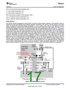
16
Submit Documentation Feedback
Copyright © 2008, Texas Instruments Incorporated
Product Folder Link(s): TPS54232

 TI [ TEXAS INSTRUMENTS ]