TPS54232
www.ti.com ........................................................................................................................................................................................... SLVS876–NOVEMBER 2008
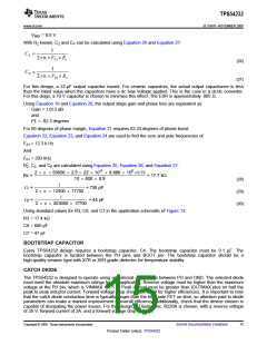
OUTPUT VOLTAGE SET POINT
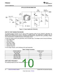
The output voltage of the TPS54232 is externally adjustable using a resistor divider network. In the application
circuit of Figure 13, this divider network is comprised of R5 and R6. The relationship of the output voltage to the
resistor divider is given by Equation 4 and Equation 5:
R5 ´ VREF
R6 =
VOUT - VREF
(4)
R5
é
ù
VOUT = VREF
´
+1
ê
ú
R6
ë
û
(5)
Choose R5 to be approximately 10.0 kΩ. Slightly increasing or decreasing R5 can result in closer output voltage
matching when using standard value resistors. In this design, R4 = 10.2 kΩ and R = 4.75 kΩ, resulting in a 2.5 V
output voltage. The zero ohm resistor R4 is provided as a convenient place to break the control loop for stability
testing.
INPUT CAPACITORS
The TPS54232 requires an input decoupling capacitor and depending on the application, a bulk input capacitor.
The typical recommended value for the decoupling capacitor is 10 µF. A high-quality ceramic type X5R or X7R is
recommended. The voltage rating should be greater than the maximum input voltage. A smaller value may be
used as long as all other requirements are met; however 10 µF has been shown to work well in a wide variety of
circuits. Additionally, some bulk capacitance may be needed, especially if the TPS54232 circuit is not located
within about 2 inches from the input voltage source. The value for this capacitor is not critical but should be rated
to handle the maximum input voltage including ripple voltage, and should filter the output so that input ripple
voltage is acceptable. For this design a 10 µF capacitor isused for the input decoupling capacitor. It isX5R
dielectric rated for 25 V. The equivalent series resistance (ESR) is approximately 5 mΩ, and the current rating is
3 A.
This input ripple voltage can be approximated by Equation 6
IOUT(MAX) ´ 0.25
DV
=
+ IOUT(MAX) ´ ESRMAX
(
)
IN
CBULK ´ fSW
(6)
Where IOUT(MAX) is the maximum load current, fSW is the switching frequency, CBULK is the input capacitor value
and ESRMAX is the maximum series resistance of the input capacitor.
The maximum RMS ripple current also needs to be checked. For worst case conditions, this can be
approximated by Equation 7
IOUT(MAX)
ICIN
=
2
(7)
In this case, the input ripple voltage would be 60 mV and the RMS ripple current would be 1 A. It is also
important to note that the actual input voltage ripple will be greatly affected by parasitics associated with the
layout and the output impedance of the voltage source. The actual input voltage ripple for this circuit is shown in
Design Parameters and is larger than the calculated value. This measured value is still below the specified input
limit of 300 mV. The maximum voltage across the input capacitors would be VIN max plus ΔVIN/2. The chosen
bulk and bypass capacitors are each rated for 25 V and the ripple current capacity is greater than 3 A, both
providing ample margin. It is very important that the maximum ratings for voltage and current are not exceeded
under any circumstance.
OUTPUT FILTER COMPONENTS
Two components need to be selected for the output filter, L1 and C3. Since the TPS54232 is an externally
compensated device, a wide range of filter component types and values can be supported.
Inductor Selection
To calculate the minimum value of the output inductor, use Equation 8
Copyright © 2008, Texas Instruments Incorporated
Submit Documentation Feedback
11
Product Folder Link(s): TPS54232

 TI [ TEXAS INSTRUMENTS ]