TPS54560
www.ti.com
SLVSBN0 –MARCH 2013
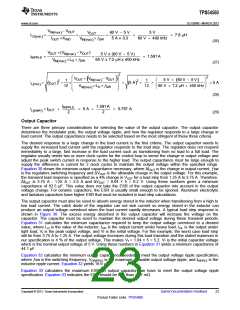
V
- VOUT
IN max
(
VOUT
)
60 V - 5 V
5 A x 0.3
5 V
LO min
=
´
=
´
= 7.6 mH
(
)
IOUT ´KIND
V
´ fSW
60 V ´ 400 kHz
IN max
(
)
(26)
(27)
spacer
IRIPPLE
V
OUT ´(V
- VOUT )
IN max
(
)
5 V x (60 V - 5 V)
=
=
= 1.591 A
V
´LO ´ fSW
60 V x 7.2 mH x 400 kHz
IN max
(
)
spacer
2
æ
ö
2
V
´ V
- V
OUT
(
OUT
)
æ
ç
ç
è
ö
÷
÷
ø
IN max
(
5 V ´ 60 V - 5 V
)
(
)
1
ç
ç
÷
1
2
2
I
=
I
(
+
´
=
5 A
+
´
= 5 A
)
( )
OUT
÷
L rms
(
)
12
V
´L ´ f
12
60 V ´ 7.2 mH ´ 400 kHz
O
SW
IN max
(
)
ç
÷
è
ø
(28)
spacer
IL peak = IOUT
IRIPPLE
1.591 A
2
+
= 5 A +
= 5.797 A
(
)
2
(29)
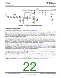
Output Capacitor
There are three primary considerations for selecting the value of the output capacitor. The output capacitor
determines the modulator pole, the output voltage ripple, and how the regulator responds to a large change in
load current. The output capacitance needs to be selected based on the most stringent of these three criteria.
The desired response to a large change in the load current is the first criteria. The output capacitor needs to
supply the increased load current until the regulator responds to the load step. The regulator does not respond
immediately to a large, fast increase in the load current such as transitioning from no load to a full load. The
regulator usually needs two or more clock cycles for the control loop to sense the change in output voltage and
adjust the peak switch current in response to the higher load. The output capacitance must be large enough to
supply the difference in current for 2 clock cycles to maintain the output voltage within the specified range.
Equation 30 shows the minimum output capacitance necessary, where ΔIOUT is the change in output current, ƒsw
is the regulators switching frequency and ΔVOUT is the allowable change in the output voltage. For this example,
the transient load response is specified as a 4% change in VOUT for a load step from 1.25 A to 3.75 A. Therefore,
ΔIOUT is 3.75 A - 1.25 A = 2.5 A and ΔVOUT = 0.04 × 5 = 0.2 V. Using these numbers gives a minimum
capacitance of 62.5 μF. This value does not take the ESR of the output capacitor into account in the output
voltage change. For ceramic capacitors, the ESR is usually small enough to be ignored. Aluminum electrolytic
and tantalum capacitors have higher ESR that must be included in load step calculations.
The output capacitor must also be sized to absorb energy stored in the inductor when transitioning from a high to
low load current. The catch diode of the regulator can not sink current so energy stored in the inductor can
produce an output voltage overshoot when the load current rapidly decreases. A typical load step response is
shown in Figure 36. The excess energy absorbed in the output capacitor will increase the voltage on the
capacitor. The capacitor must be sized to maintain the desired output voltage during these transient periods.
Equation 31 calculates the minimum capacitance required to keep the output voltage overshoot to a desired
value, where LO is the value of the inductor, IOH is the output current under heavy load, IOL is the output under
light load, Vf is the peak output voltage, and Vi is the initial voltage. For this example, the worst case load step
will be from 3.75 A to 1.25 A. The output voltage increases during this load transition and the stated maximum in
our specification is 4 % of the output voltage. This makes Vf = 1.04 × 5 = 5.2. Vi is the initial capacitor voltage
which is the nominal output voltage of 5 V. Using these numbers in Equation 31 yields a minimum capacitance of
44.1 μF.
Equation 32 calculates the minimum output capacitance needed to meet the output voltage ripple specification,
where ƒsw is the switching frequency, VORIPPLE is the maximum allowable output voltage ripple, and IRIPPLE is the
inductor ripple current. Equation 32 yields 19.9 μF.
Equation 33 calculates the maximum ESR an output capacitor can have to meet the output voltage ripple
specification. Equation 33 indicates the ESR should be less than 15.7 mΩ.
Copyright © 2013, Texas Instruments Incorporated
Submit Documentation Feedback
23
Product Folder Links: TPS54560

 TI [ TEXAS INSTRUMENTS ]