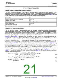
TPS54560
www.ti.com
SLVSBN0 –MARCH 2013
2
)
V
(
- V
´ I
´ Vf d
OUT
)
IN max
OUT
C ´ f
´ V + Vf d
(
IN max
(
)
j
SW
IN
P =
+
=
D
V
2
(
)
2
60 V - 5 V ´ 5 A x 0.7 V
(
)
60 V
300 pF x 400 kHz x (60 V + 0.7 V)
+
= 3.43 W
2
(35)
Input Capacitor
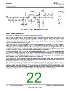
The TPS54560 requires a high quality ceramic type X5R or X7R input decoupling capacitor with at least 3 μF of
effective capacitance. Some applications will benefit from additional bulk capacitance. The effective capacitance
includes any loss of capacitance due to dc bias effects. The voltage rating of the input capacitor must be greater
than the maximum input voltage. The capacitor must also have a ripple current rating greater than the maximum
input current ripple of the TPS54560. The input ripple current can be calculated using Equation 36.
The value of a ceramic capacitor varies significantly with temperature and the dc bias applied to the capacitor.
The capacitance variations due to temperature can be minimized by selecting a dielectric material that is more
stable over temperature. X5R and X7R ceramic dielectrics are usually selected for switching regulator capacitors
because they have a high capacitance to volume ratio and are fairly stable over temperature. The input capacitor
must also be selected with consideration for the dc bias. The effective value of a capacitor decreases as the dc
bias across a capacitor increases.
For this example design, a ceramic capacitor with at least a 60 V voltage rating is required to support the
maximum input voltage. Common standard ceramic capacitor voltage ratings include 4 V, 6.3 V, 10 V, 16 V, 25
V, 50 V or 100 V. For this example, four 2.2 μF, 100 V capacitors in parallel are used. Table 2 shows several
choices of high voltage capacitors.
The input capacitance value determines the input ripple voltage of the regulator. The input voltage ripple can be
calculated using Equation 37. Using the design example values, IOUT = 5 A, CIN = 8.8 μF, ƒsw = 400 kHz, yields
an input voltage ripple of 355 mV and a rms input ripple current of 2.26 A.
V
- V
OUT
)
= 5 A
(
IN min
(
7 V - 5 V
)
V
(
)
5 V
7 V
OUT
I
= I
x
x
´
= 2.26 A
OUT
CI rms
(
)
V
V
7 V
IN min
(
IN min
(
)
)
(36)
(37)
I
´ 0.25
5 A ´ 0.25
8.8 mF ´ 400 kHz
OUT
DV
=
=
= 355 mV
IN
C
´ f
IN
SW
Table 2. Capacitor Types
VENDOR
VALUE (μF)
1 to 2.2
1 to 4.7
1
EIA Size
VOLTAGE
100 V
50 V
DIALECTRIC
COMMENTS
1210
GRM32 series
Murata
100 V
50 V
1206
2220
2225
1812
1210
1210
1812
GRM31 series
VJ X7R series
1 to 2.2
1 to 1.8
1 to 1.2
1 to 3.9
1 to 1.8
1 to 2.2
1.5 to 6.8
1 to 2.2
1 to 3.3
1 to 4.7
1
50 V
100 V
50 V
Vishay
TDK
100 V
100 V
50 V
X7R
C series C4532
C series C3225
100 V
50 V
50 V
100 V
50 V
AVX
X7R dielectric series
1 to 4.7
1 to 2.2
100 V
Copyright © 2013, Texas Instruments Incorporated
Submit Documentation Feedback
25
Product Folder Links: TPS54560

 TI [ TEXAS INSTRUMENTS ]