TPS51216
www.ti.com
SLUSAB9 –NOVEMBER 2010
•
•
•
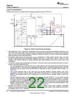
Connect the overcurrent setting resistors from TRIP pin to ground and make the connections as close as
possible to the device. The trace from TRIP pin to resistor and from resistor to ground should avoid coupling
to a high-voltage switching node.
Connect the frequency and mode setting resistor from MODE pin to ground, and make the connections as
close as possible to the device. The trace from the MODE pin to the resistor and from the resistor to ground
should avoid coupling to a high-voltage switching node
Connections from gate drivers to the respective gate of the high-side or the low-side MOSFET should be as
short as possible to reduce stray inductance. Use 0.65 mm (25 mils) or wider trace and via(s) of at least 0.5
mm (20 mils) diameter along this trace.
•
•
•
•
The PCB trace defined as SW node, which connects to the source of the switching MOSFET, the drain of the
rectifying MOSFET and the high-voltage side of the inductor, should be as short and wide as possible.
VLDOIN should be connected to VDDQ output with short and wide traces. An input bypass capacitor should
be placed as close as possible to the pin with short and wideꢀconnections.
The output capacitor for VTT should be placed close to the pin with a short and wide connection in order
toꢀavoid additional ESR and/or ESL of the trace.
VTTSNS should be connected to the positive node of the VTT output capacitor(s) as a separate trace from
the high-current power line and is strongly recommended to avoid additional ESR and/or ESL. If it is needed
toꢀsense the voltage at the point of the load, it is recommended to attach the output capacitor(s) at that
point. Also, it is recommended to minimize any additional ESR and/or ESL of ground trace between GND pin
and the output capacitor(s).
•
•
•
•
Consider adding a low pass filter (LPF) at VTTSNS in case the ESR of the VTT output capacitor(s) is larger
than 2 mΩ.
VDDQSNS can be connected separately from VLDOIN. Remember that this sensing potential is the
referenceꢀvoltage of VTTREF. Avoid any noise generative lines.
The negative node of the VTT output capacitor(s) and the VTTREF capacitor should be tied together by
avoidingꢀcommon impedance to high-current path of the VTT source/sink current.
GND pin node represents the reference potential for VTTREF and VTT outputs. Connect GNDꢀto negative
nodes of VTT capacitor(s), VTTREF capacitor and VDDQ capacitor(s) with care to avoid additional ESR
and/or ESL. GND and PGND should be connected together at a single point.
•
In order to effectively remove heat from the package, prepare the thermal land and solder to the
packageꢀthermal pad. Wide trace of the component-side copper, connected to this thermal land, helps heat
spreading.ꢀNumerous vias with a 0.3-mm diameter connected from the thermal land to the internal/solder-
side groundꢀplane(s) should be used to help dissipation.
CAUTION
Do NOT connect PGND pin directly to this thermal land underneath the package.
Copyright © 2010, Texas Instruments Incorporated
Submit Documentation Feedback
23
Product Folder Link(s) :TPS51216

 TI [ TEXAS INSTRUMENTS ]