TPS51640A, TPS59640, TPS59641
www.ti.com
SLUSAQ2 –JANUARY 2012
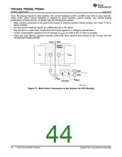
Minimize High-Current Loops
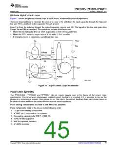
Figure 73 shows the primary current loops in each phase, numbered in order of importance.
The most important loop to minimize the area of is Loop 1, the path from the input capacitor through the high and
low side FETs, and back to the capacitor through ground.
Loop 2 is from the inductor through the output capacitor, ground and Q2. The layout of the low side gate drive
(Loops 3a and 3b) is important. The guidelines for gate drive layout are:
•
•
•
Make the low-side gate drive as short as possible (1 inch or less preferred).
Make the DRVL width to length ratio of 1:10, wider (1:5) if possible.
If changing layers is necessary, use at least two vias.
VBAT
CB
CIN
1
Q1
4b
DRVH
4a
L
VCORE
LL
2
Q2
CD
DRVL
3a
COUT
3b
PGND
UDG-11040
Figure 73. Major Current Loops to Minimize
Power Chain Symmetry
The TPS51640A, TPS59640, and TPS59641 do not require special care in the layout of the power chain
components. This is because independent isolated current feedback is provided. If it is possible to lay out the
phases in a symmetrical manner, then please do so. The rule is: the current feedback from each phase needs to
be clean of noise and have the same effective current sense resistance.
Place analog components as close to the device as possible.
Place components close to the device in the following order.
1. CS pin noise filtering components
2. xCOMP pin compensation components
3. Decoupling capacitors for VREF, V3R3, V5
4. xTHERM filter capacitor
5. xIMON capacitor, resistors
6. xF-IMAX resistors
Copyright © 2012, Texas Instruments Incorporated
Submit Documentation Feedback
45

 TI [ TEXAS INSTRUMENTS ]