TPS40200-Q1
www.ti.com
SLUS739D –SEPTEMBER 2006–REVISED JULY 2011
MOSFET Gate Drive
The output driver sinking current is approximately 200 mA and is designed to drive P-channel power FETs. When
the driver pulls the gate charge of the FET it is controlling to –8 V, the drive current folds back to a low level so
that high power dissipation only occurs during the turn-on period of the FET. This feature is particularly valuable
when turning on a FET at high input voltages, where leaving the gate drive current on would otherwise cause
unacceptable power dissipation.
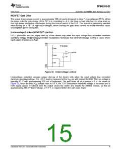
Undervoltage Lockout (UVLO) Protection
UVLO protection ensures proper start-up of the device only when the input voltage has exceeded minimum
operating voltage. Undervoltage protection incorporates hysteresis that eliminates hiccup starting in cases where
input supply impedance is high.
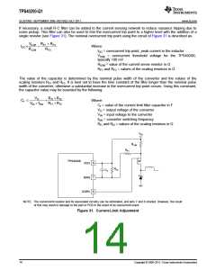
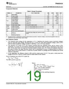
VDD
8
TPS40200
545k
-
RUN
+
200K
+
1.3V
36K
GND
5
Figure 32. Undervoltage Lockout
Undervoltage protection ensures proper start-up of the device only when the input voltage has exceeded
minimum operating voltage. The UVLO level is measured at the VDD pin with respect to GND. Start-up voltage is
typically 4.3 V with approximately 200 mV of hysteresis. The part shuts off at a nominal 4.1 V. As shown in
Figure 32, when the input VDD voltage rises to 4.3 V, the 1.3-V comparator threshold voltage is exceeded and a
RUN signal occurs. Feedback from the output closes the switch and shunts the 200-kΩ resistor, so that an
approximately 200-mV lower voltage, or 4.1 V, is required before the part shuts down.
Copyright © 2006–2011, Texas Instruments Incorporated
15

 TI [ TEXAS INSTRUMENTS ]