TPS3808-Q1
SBVS085H –JANUARY 2007–REVISED JUNE 2012
www.ti.com
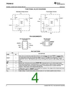
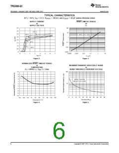
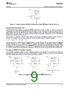
FUNCTIONAL BLOCK DIAGRAMS
Adjustable-Voltage Version
Fixed-Voltage Versions
VDD
VDD
VDD
VDD
90k
90k
RESET
RESET
MR
MR
Reset
Logic
Timer
SENSE
Reset
Logic
Timer
R1
−
−
SENSE
CT
CT
+
+
R2
0.4 V
VREF
0.4 V
VREF
R1 + R2 = 4 MW
GND
GND
PIN ASSIGNMENTS
DBV (SOT-23) PACKAGE
(TOP VIEW)
DRV PACKAGE
(TOP VIEW)
VDD
SENSE
CT
1
2
3
6
5
4
RESET
GND
MR
6
5
4
1
2
3
RESET
GND
MR
VDD
SENSE
CT
PIN FUNCTIONS
PIN
DESCRIPTION
NAME
NO.
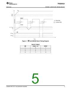
Reset. This is an open-drain output that is driven to a low impedance state when RESET is asserted (either
the SENSE input is lower than the threshold voltage (VIT) or the MR pin is set to a logic low). RESET remains
low (asserted) for the reset period after both SENSE is above VIT and MR is set to a logic high. A pullup
resistor from 10 kΩ to 1 MΩ should be used on this pin, and allows the reset pin to attain voltages higher than
RESET
1
VDD
.
GND
MR
2
3
Ground
Manual reset. Driving this pin low asserts RESET. MR is internally tied to VDD by a 90-kΩ pullup resistor.
Reset period programming. Connecting this pin to VDD through a 40-kΩ to 200-kΩ resistor or leaving it open
results in fixed delay times (see Electrical Characteristics). Connecting this pin to a ground referenced
capacitor ≥ 100 pF gives a user-programmable delay time.
CT
4
Voltage sense. This pin is connected to the voltage to be monitored. If the voltage at this terminal drops below
the threshold voltage (VIT), RESET is asserted.
SENSE
VDD
5
6
Supply voltage. It is good analog design practice to place a 0.1-μF ceramic capacitor close to this pin.
4
Copyright © 2007–2012, Texas Instruments Incorporated

 TI [ TEXAS INSTRUMENTS ]