TPS3808-Q1
SBVS085H –JANUARY 2007–REVISED JUNE 2012
www.ti.com
DEVICE OPERATION
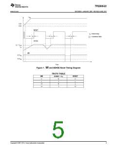
The TPS3808 microprocessor supervisory product family is designed to assert a RESET signal when either the
SENSE pin voltage drops below VIT or the manual reset (MR) is driven low. The RESET output remains asserted
for a user-adjustable time after both the manual reset (MR) and SENSE voltages return above the respective
thresholds. A broad range of voltage threshold and reset delay time adjustments are available, allowing these
devices to be used in a wide array of applications. Reset threshold voltages can be factory-set from 0.82 V to
3.3 V or from 4.4 V to 5.0 V, while the TPS3808G01 can be set to any voltage above 0.405 V using an external
resistor divider. Two preset delay times are also user-selectable: connecting the CT pin to VDD results in a 300-
ms reset delay, while leaving the CT pin open yields a 20-ms reset delay. In addition, connecting a capacitor
between CT and GND allows the designer to select any reset delay period from 1.25 ms to 10 s.
SENSE Input
The SENSE input provides a terminal at which any system voltage can be monitored. If the voltage on this pin
drops below VIT, RESET is asserted. The comparator has a built-in hysteresis to ensure smooth RESET
assertions and deassertions. It is good analog design practice to put a 1-nF to 10-nF bypass capacitor on the
SENSE input to reduce sensitivity to transients and layout parasitics.
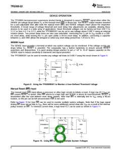
The TPS3808G01 can be used to monitor any voltage rail down to 0.405 V using the circuit shown in Figure 9.
VIN
VOUT
VDD
R1
R2
VIT
′
= (1 +
)0.405
R1
TPS3808G01
SENSE
RESET
GND
R2
1nF
Figure 9. Using the TPS3808G01 to Monitor a User-Defined Threshold Voltage
Manual Reset (MR) Input
The manual reset (MR) input allows a processor or other logic circuits to initiate a reset. A logic low (0.3 VDD) on
MR causes RESET to assert. After MR returns to a logic high and SENSE is above its reset threshold, RESET is
deasserted after the user-defined reset delay expires. Note that MR is internally tied to VDD using a 90-kΩ
resistor, so this pin can be left unconnected if MR is not used.
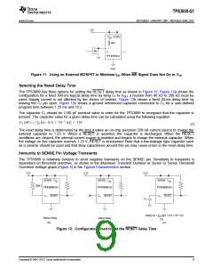
Refer to Figure 10 for how MR can be used to monitor multiple system voltages. Note that if the logic signal
driving MR does not go fully to VDD, there will be some additional current draw into VDD as a result of the internal
pullup resistor on MR. To minimize current draw, a logic-level FET can be used as shown in Figure 11.
1.2V
3.3V
V
V
CORE
SENSE
V
SENSE V
DD
I/O
DD
TPS3808G12
TPS3808G33
DSP
RESET
MR
RESET
GPIO
GND
CT
CT
GND
GND
Figure 10. Using MR to Monitor Multiple System Voltages
8
Copyright © 2007–2012, Texas Instruments Incorporated

 TI [ TEXAS INSTRUMENTS ]