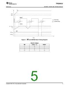
TPS3808-Q1
SBVS085H –JANUARY 2007–REVISED JUNE 2012
www.ti.com
This integrated circuit can be damaged by ESD. Texas Instruments recommends that all integrated circuits be handled with
appropriate precautions. Failure to observe proper handling and installation procedures can cause damage.
ESD damage can range from subtle performance degradation to complete device failure. Precision integrated circuits may be more
susceptible to damage because very small parametric changes could cause the device not to meet its published specifications.
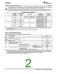
ORDERING INFORMATION(1)
NOMINAL
SUPPLY
VOLTAGE
THRESHOLD
VOLTAGE
(VIT)
ORDERABLE
PART NUMBER
TOP-SIDE
MARKING
TJ
PACKAGE(2)
SON – DRV Reel of 3000
TPS3808G01QDRVRQ1 PSJQ
TPS3808G01QDBVRQ1 BAZ
TPS3808G125QDBVRQ1 QWZ
TPS3808G12QDBVRQ1 CEM
TPS3808G15QDBVRQ1 OFR
TPS3808G18QDBVRQ1 OBZ
TPS3808G30QDBVRQ1 AVP
TPS3808G33QDBVRQ1 AVQ
TPS3808G50QDBVRQ1 CEL
Adjustable
0.405 V
SOT-23 – DBV Reel of 3000
SOT-23 – DBV Reel of 3000
1.25 V
1.2 V
1.5 V
1.8 V
3 V
1.16 V
1.12 V
1.4 V
–40°C to 125°C
1.67 V
2.79 V
3.07 V
4.65 V
3.3 V
5 V
(1) For the most current package and ordering information, see the Package Option Addendum at the end of this document, or see the TI
web site at www.ti.com.
(2) Package drawings, thermal data, and symbolization are available at www.ti.com/packaging.
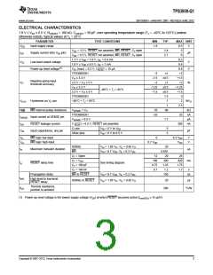
ABSOLUTE MAXIMUM RATINGS
over operating junction temperature range (unless otherwise noted)(1)
VDD
VCT
VMR
Input voltage range
CT voltage range
–0.3 V to 7 V
–0.3 V to (VDD + 0.3) V
,
VRESET
,
MR, RESET, SENSE voltage ranges
–0.3 V to 7 V
VSENSE
IRESET
TJ
RESET pin current
Operating junction temperature range(2)
5 mA
–40°C to 150°C
–65°C to 150°C
2 kV
Tstg
Storage temperature range
Human-Body Model (HBM)
TPS3808GXX
500 V
Charged-Device Model (CDM)
ESD
Electrostatic discharge rating
TPS3808G125QDBVRQ1
1000 V
Machine Model (MM),
TPS3808G01QDRVRQ1,TPS3808G125QDBVRQ1
50 V
(1) Stresses beyond those listed under Absolute Maximum Ratings may cause permanent damage to the device. These are stress ratings
only, and functional operation of the device at these or any other conditions beyond those indicated under the Electric Characteristics is
not implied. Exposure to absolute-maximum-rated conditions for extended periods may affect device reliability.
(2) Due to the low dissipated power in this device, it is assumed that TJ = TA.
2
Copyright © 2007–2012, Texas Instruments Incorporated

 TI [ TEXAS INSTRUMENTS ]