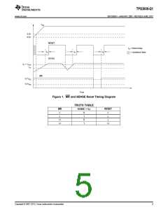
TPS3808-Q1
www.ti.com
SBVS085H –JANUARY 2007–REVISED JUNE 2012
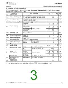
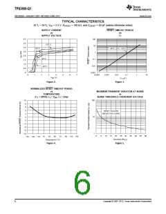
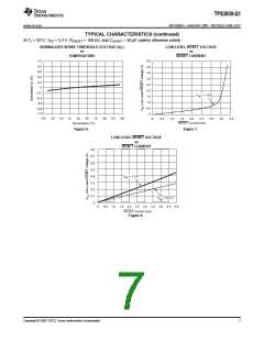
ELECTRICAL CHARACTERISTICS
1.8 V ≤ VDD ≤ 6.5 V, RLRESET = 100 kΩ, CLRESET = 50 pF, over operating temperature range (TJ = –40°C to 125°C) (unless
otherwise noted), typical values at TJ = 25°C
PARAMETER
TEST CONDITIONS
MIN
TYP
MAX UNIT
VDD
IDD
Input supply range
1.8
6.5
5
V
VDD = 3.3 V, RESET not asserted, MR, RESET, CT open
VDD = 6.5 V, RESET not asserted, MR, RESET, CT open
1.3 V ≤ VDD < 1.8 V, IOL = 0.4 mA
2.4
2.7
Supply current (into VDD pin)
μA
6
0.3
0.4
0.8
+2
VOL
Low-level output voltage
Power-up reset voltage(1)
V
V
1.8 V ≤ VDD ≤ 6.5 V, IOL = 1 mA
VOL (max) = 0.2 V, I RESET = 15 μA
TPS3808G01
–2
–1.5
–2
±1
±0.5
±1
V
IT ≤ 3.3 V
3.3 V < VIT ≤ 5 V
IT ≤ 3.3 V
+1.5
+2
Negative-going input
threshold accuracy
VIT
%
V
–1.25
–1.5
±0.5
±0.5
1.5
1
+1.25
+1.5
3
–40°C < TJ < 85°C
3.3 V < VIT ≤ 5 V
TPS3808G01
VHYS
Hysteresis on VIT pin
–40°C < TJ < 85°C
2
%VIT
1
2.5
RMR
MR internal pullup resistance
VSENSE = VIT
TPS3808G01
VSENSE = 6.5 V
70
90
kΩ
nA
μA
nA
–25
25
ISENSE Input current at SENSE pin
1.7
IOH
CIN
RESET leakage current
V RESET = 6.5 V, RESET not asserted
300
CT pin
VIN = 0 V to VDD
VIN = 0 V to 6.5 V
5
5
Input capacitance, any pin
pF
Other pins
VIL
VIH
MR logic low input
MR logic high input
0
0.3 VDD
VDD
V
V
0.7 VDD
SENSE
VIH = 1.05 VIT, VIL = 0.95 VIT
VIH = 0.7 VDD, VIL = 0.3 VDD
20
0.001
20
tw
Maximum transient duration
μs
MR
CT = Open
CT = VDD
CT = 100 pF
CT = 180 nF
MR to RESET
12
180
0.75
0.7
28
420
1.75
1.7
300
1.25
1.2
ms
td
RESET delay time
Propagation delay
See timing diagram
s
VIH = 0.7 VDD, VIL = 0.3 VDD
VIH = 1.05 VIT, VIL = 0.95 VIT
150
ns
tpHL
High-level to low-level
RESET delay
SENSE to RESET
20
μs
Thermal resistance,
junction to ambient
θJA
290
°C/W
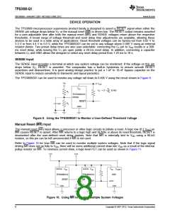
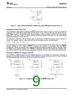
(1) Power-up reset voltage is the lowest supply voltage (VDD) at which RESET becomes active (trise(VDD) ≥ 15 μs/V).
Copyright © 2007–2012, Texas Instruments Incorporated
3

 TI [ TEXAS INSTRUMENTS ]