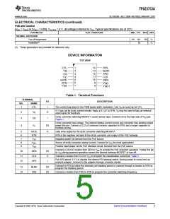
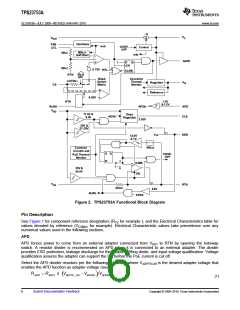
TPS23753A
www.ti.com
SLVS933B –JULY 2009–REVISED JANUARY 2010
RECOMMENDED OPERATING CONDITIONS
Voltage with respect to VSS (unless otherwise noted)
MIN
0
NOM
MAX
57
18
VB
2
UNIT
V
Input voltage range, VDD, VDD1, RTN
Input voltage range, VC to RTN
0
V
VI
Input voltage range, APD, CTL to RTN
0
V
Input voltage range, CS to RTN
RTN current (TJ ≤ 125°C)
VB sourcing current
0
V
350
5
mA
mA
mF
kΩ
ns
°C
0
0.08
0
2.5
VB capacitance
0..1
RBLNK
350
125
Synchronization pulse width input (when used)
25
TJ
Operating junction temperature range
–40
ELECTRICAL CHARACTERISTICS
Unless otherwise noted: CS = APD = CTL = RTN, GATE open, RFRS = 60.4 kΩ, RBLNK = 249 kΩ, CVB = CVC = 0.1 mF, RDEN
24.9 kΩ, RCLS open, VVDD-VSS = 48 V, VVDD1-RTN = 48 V, 8.5 V ≤ VVC-RTN ≤ 18 V, –40°C ≤ TJ ≤ 125°C
Controller Section Only
=
[VSS = RTN and VDD = VDD1] or [VSS = RTN = VDD], all voltages referred to RTN. Typical specifications are at 25°C.
PARAMETER
TEST CONDITIONS
MIN
TYP
MAX UNIT
VC
UVLO_1
UVLO_H
VC rising
Hysteresis(1)
8.65
3.3
9
3.5
9.3
3.7
Undervoltage lockout
Operating current
V
VC = 12 V, CTL = VB
0.40
50
0.58
85
0.85
175
85
mA
ms
VDD1 = 10.2 V, VVC(0) = 0 V
VDD1 = 35 V, VVC(0) = 0 V
VDD1 = 10.2 V, VVC = 8.6 V
VDD1 = 48 V, VVC = 0 V
tST
Startup time, CVC = 22 mF
30
48
0.44
2.5
1.06
4.3
1.80
6.0
Startup current source - IVC
Voltage
mA
V
VB
6.5 V ≤ VC ≤ 18 V, 0 ≤ IVB ≤ 5 mA
4.75
223
5.10
5.25
273
FRS
CTL= VB, Measure GATE
Switching frequency
248
kHz
RFRS = 60.4 kΩ
78.5
%
DMAX
Duty cycle
CTL= VB, Measure GATE
Input threshold
76%
2
81%
2.4
VSYNC
CTL
Synchronization
2.2
V
VZDC
0% duty cycle threshold
Softstart period
V
CTL ↓ until GATE stops
1.3
400
70
1.5
800
100
1.7
V
Interval from switching start to VCSMAX
ms
kΩ
Input resistance
145
BLNK
In addition to t1
BLNK = RTN
Blanking delay
35
41
52
52
75
63
ns
RBLNK = 49.9 kΩ
CS
VCSMAX
t1
VSLOPE
ISL_EX
Maximum threshold voltage
Turn off delay
VCTL = VB, VCS ↑ until GATE duty cycle drops
VCS = 0.65 V
0.50
25
90
30
2
0.55
41
0.60
60
V
ns
Internal slope compensation voltage
Peak slope compensation current
Bias current (sourcing)
Peak voltage at maximum duty cycle, referred to CS
VCTL = VB, ICS at maximum duty cycle (ac component)
Gate high, dc component of CS current
118
42
142
54
mV
mA
mA
3
4.2
(1) The hysteresis tolerance tracks the rising threshold for a given device.
Copyright © 2009–2010, Texas Instruments Incorporated
Submit Documentation Feedback
3

 TI [ TEXAS INSTRUMENTS ]