TPS23753A
SLVS933B –JULY 2009–REVISED JANUARY 2010
www.ti.com
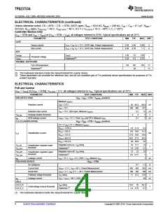
FRS
Connect a resistor from FRS to RTN to program the converter switching frequency. Select the resistor per the
following relationship.
15000
R
(kΩ) =
FRS
f
(kHz)
SW
(4)
The converter may be synchronized to a frequency above its maximum free-running frequency by applying short
ac-coupled pulses into the FRS pin. More information is provided in the Applications section.
The FRS pin is high impedance. Keep the connections short and apart from potential noise sources.
GATE
Gate drive output for the dc/dc converter switching MOSFET.
RTN
RTN is internally connected to the drain of the PoE hotswap MOSFET, and the dc/dc controller return. RTN
should be treated as a local reference plane (ground plane) for the dc/dc controller and converter primary to
maintain signal integrity.
VB
VB is an internal 5V control rail that should be bypassed by a 0.1 mF capacitor to RTN. VB should be used to bias
the feedback optocoupler.
VC
VC is the bias supply for the dc/dc controller. The MOSFET gate driver runs directly from VC. VB is regulated
down from VC, and is the bias voltage for the rest of the converter control. A startup current source from VDD1 to
VC is controlled by a comparator with hysteresis to implement a bootstrap startup of the converter. VC must be
connected to a bias source, such as a converter auxiliary output, during normal operation.
A minimum 0.22 mF capacitor, located adjacent to the VC pin, should be connected from VC to RTN to bypass the
gate driver. A larger total capacitance is required for startup.
VDD
Positive input power rail for PoE control that is derived from the PoE. VDD should be bypassed to VSS with a 0.1
mF (X7R,10%) capacitor as required by the standard. A transient suppressor (Zener) diode, should be connected
from VDD to VSS to protect against overvoltage transients.
VDD1
Source of dc/dc converter startup current. Connect to VDD for most applications. VDD1 may be isolated by a diode
from VDD to support PoE priority operation.
VSS
VSS is the PoE input-power return side. It is the reference for the PoE interface circuits, and has a current-limited
hotswap switch that connects it to RTN. VSS is clamped to a diode drop above RTN by the hotswap switch. A
local VSS reference plane should be used to connect the input components and the VSS pin.
8
Submit Documentation Feedback
Copyright © 2009–2010, Texas Instruments Incorporated

 TI [ TEXAS INSTRUMENTS ]