TPS23753A
SLVS933B –JULY 2009–REVISED JANUARY 2010
www.ti.com
This integrated circuit can be damaged by ESD. Texas Instruments recommends that all integrated circuits be handled with
appropriate precautions. Failure to observe proper handling and installation procedures can cause damage.
ESD damage can range from subtle performance degradation to complete device failure. Precision integrated circuits may be more
susceptible to damage because very small parametric changes could cause the device not to meet its published specifications.
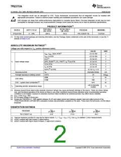
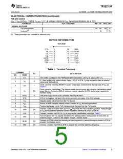
PRODUCT INFORMATION(1)
POE UVLO
ON / HYST.
DC/DC UVLO
ON / HYST.
DEVICE
DUTY CYCLE
PACKAGE
MARKING
TPS23753A
0 – 78%
35/4.5
9/3.5
PW (TSSOP-14)
T23753A
(1) For the most current package and ordering information, see the Package Option Addendum at the end of this document, or see the TI
website at www.ti.com.
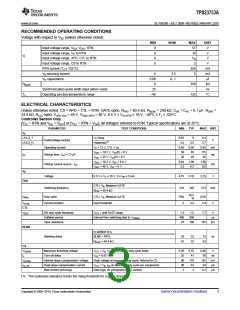
ABSOLUTE MAXIMUM RATINGS(1)
Voltage are with respect to VSS (unless otherwise noted)
VALUE
–0.3 to 100
–0.3 to 100
–0.3 to 6.5
–0.3 to 6.5
–0.3 to VB
–0.3 to 19
–0.3 to VC + 0.3
Internally limited
25
UNIT
VDD, VDD1, DEN, RTN(2)
V
V
VDD1 to RTN
CLS(3)
[APD, BLNK(3), CTL, FRS(3), VB (3)] to RTN
V
VI
Input voltage range
V
CS to RTN
VC to RTN
GATE(3) to RTN
VB
V
V
V
Sourcing current
mA
mARMS
kV
V
Average sourcing or sinking current
GATE
HBM
2
ESD rating
CDM
500
ESD – system level (contact/air)(4)
Operating junction temperature range
8/15
kV
–40 to Internally
Limited
TJ
°C
(1) Stresses beyond those listed under absolute maximum ratings may cause permanent damage to the device. These are stress ratings
only, and functional operation of the device at these or any other conditions beyond those indicated under recommended operating
conditions is not implied. Exposure to absolute-maximum-rated conditions for extended periods may affect device reliability.
(2) IRTN = 0 for VRTN > 80V.
(3) Do not apply voltage to these pins.
(4) Surges per EN61000-4-2, 1999 applied between RJ-45 and output ground and between adapter input and output ground of the
TPS23753AEVM-001 (HPA304-001) evaluation module (documentation available on the web). These were the test levels, not the failure
threshold.
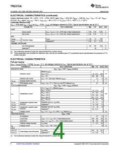
DISSIPATION RATINGS
yJT
qJA
qJA
PACKAGE
(°C/W)(1)
(°C/W)(2)
(°C/W)(3)
PW (TSSOP-14)
0.97
173.6
99.3
(1) Thermal resistance junction to case top for high-k boards. TJ = TTOP + (yJT x PJ). Use yJT to validate TJ from measurements.
(2) JEDEC method with low-k board (2 signal layers).
(3) JEDEC method with high-k board (4 layers, 2 signal and 2 planes).
2
Submit Documentation Feedback
Copyright © 2009–2010, Texas Instruments Incorporated

 TI [ TEXAS INSTRUMENTS ]