TPS23753A
www.ti.com
SLVS933B –JULY 2009–REVISED JANUARY 2010
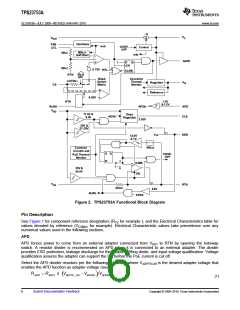
R
APD1 + R
APD2
V
=
x V
(
-V
)
ADPTR _ OFF
APDEN APDH
R
APD2
(2)
The CLS output is disabled when a voltage above VAPDEN is applied to the APD pin.
Place the APD pull-down resistor adjacent to the APD pin.
APD should be tied to RTN when not used.
BLNK
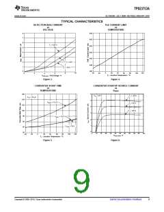
Blanking provides an interval between the gate drive going high and the current comparator on CS actively
monitoring the input. This delay allows the normal turn-on current transient (spike) to subside before the
comparator is active, preventing undesired short duty cycles and premature current limiting.
Connect BLNK to RTN to obtain the internally set blanking period. Connect a resistor from BLNK to RTN for a
programmable blanking period. The relationship between the desired blanking period and the programming
resistor is defined by the following equation.
R
kΩ = t
( )
ns
BLNK
( )
BLNK
(3)
Place the resistor adjacent to the BLNK pin when it is used.
CLS
Connect a resistor from CLS to VSS to program the classification current per IEEE 802.3-at. The PD power
ranges and corresponding resistor values are listed in Table 2. The power assigned should correspond to the
maximum average power drawn by the PD during operation. The TPS23753A supports class 0 – 3 power levels.
CS
The current sense input for the dc/dc converter should be connected to the high side of the switching MOSFET’s
current sense resistor. The current-limit threshold, VCSMAX, defines the voltage on CS above which the GATE ON
time are terminated regardless of the voltage on CTL.
The TPS23753A provides internal slope compensation to stabilize the current mode control loop. If the provided
slope is not sufficient, the effective slope may be increased by addition of RS per Figure 22.
Routing between the current-sense resistor and the CS pin should be short to minimize cross-talk from noisy
traces such as the gate drive signal.
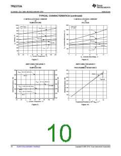
CTL
CTL is the voltage control loop input to the PWM (pulse width modulator). Pulling VCTL below VZDC causes GATE
to stop switching. Increasing VCTL above VZDC raises the switching MOSFET programmed peak current. The
maximum (peak) current is requested at approximately VZDC + (2 × VCSMAX). The ac gain from CTL to the PWM
comparator is 0.5.
Use VB as a pull up source for CTL.
DEN
Connect a 24.9 kΩ resistor from DEN to VDD to provide the PoE detection signature. DEN goes to a high
impedance state when not in the detection voltage range. Pulling DEN to VSS during powered operation causes
the internal hotswap MOSFET and class regulator to turn off.
Copyright © 2009–2010, Texas Instruments Incorporated
Submit Documentation Feedback
7

 TI [ TEXAS INSTRUMENTS ]