TPS1HC30-Q1
ZHCSP75A –JULY 2022 –REVISED DECEMBER 2022
www.ti.com.cn
»
ÿ
Ÿ
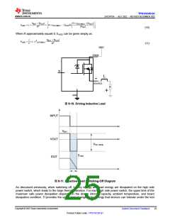
VBAT + VOUT
≈ R ì IOUT(MAX) + VOUT
’
…
ì R ì IOUT(MAX) œ VOUT ln
EHSD = L ì
∆
÷
÷
◊
R2
∆
VOUT
…
Ÿ
⁄
«
(10)
(11)
When R approximately equals 0, EHSD can be given simply as:
VBAT + VOUT
1
2
EHSD
=
ì L ì I2
OUT(MAX)
R2
VBAT
DRAIN
IN
L
-
-
SOURCE
+
GND
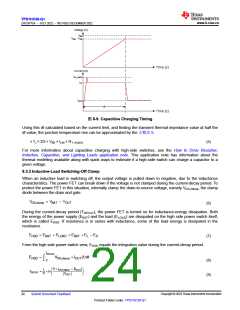
图8-10. Driving Inductive Load
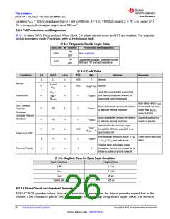
INPUT
VBAT
VOUT
IOUT
VDS, clamp
EHSD
tDECAY
图8-11. Inductive-Load Switching-Off Diagram
As discussed previously, when switching off, battery energy and load energy are dissipated on the high side
power switch, which leads to the large thermal variation. For each high side power switch, the upper limit of the
maximum safe power dissipation depends on the device intrinsic capacity, ambient temperature, and board
dissipation condition. TI provides the upper limit of single-pulse energy that devices can tolerate under the test
Copyright © 2023 Texas Instruments Incorporated
Submit Document Feedback
25
Product Folder Links: TPS1HC30-Q1

 TI [ TEXAS INSTRUMENTS ]