TPS1HC30-Q1
ZHCSP75A –JULY 2022 –REVISED DECEMBER 2022
www.ti.com.cn
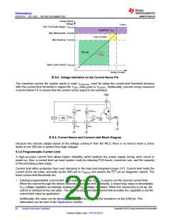
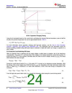
Voltage (V)
VBB
VBB - VDS
Time (s)
Current (A)
ICL_ENPS
ICL
INOM
dt
Time (s)
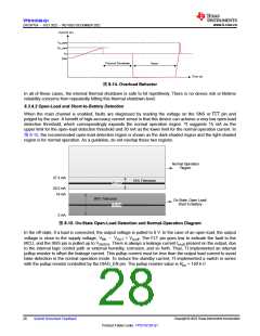
图8-9. Capacitive Charging Timing
Using this dt calculated based on the current limit, and finding the transient thermal impedance value at half the
dt value, the junction temperature rise can be approximated by the 方程式5.
ΔTJ ≅ 2/3 × VBB × ILIM × RθJA(dt/2)
(5)
For more information about capacitive charging with high-side switches, see the How to Drive Resistive,
Inductive, Capacitive, and Lighting Loads application note. This application note has information about the
thermal modeling available along with quick ways to estimate if a high-side switch can charge a capacitor to a
given voltage.
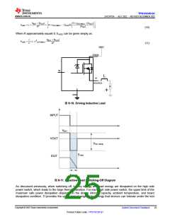
8.3.3 Inductive-Load Switching-Off Clamp
When an inductive load is switching off, the output voltage is pulled down to negative, due to the inductance
characteristics. The power FET can break down if the voltage is not clamped during the current-decay period. To
protect the power FET in this situation, internally clamp the drain-to-source voltage, namely VDS,clamp, the clamp
diode between the drain and gate.
VDS,clamp = VBAT œ VOUT
(6)
During the current-decay period (TDECAY), the power FET is turned on for inductance-energy dissipation. Both
the energy of the power supply (EBAT) and the load (ELOAD) are dissipated on the high side power switch itself,
which is called EHSD. If resistance is in series with inductance, some of the load energy is dissipated in the
resistance.
EHSD = EBAT + ELOAD = EBAT +EL œ ER
(7)
From the high side power switch view, EHSD equals the integration value during the current-decay period.
TDECAY
EHSD
=
VDS,clamp ì IOUT(t)dt
—
0
(8)
(9)
≈
’
R ì IOUT(MAX) + VOUT
L
∆
∆
«
÷
÷
◊
TDECAY
=
ì ln
R
VOUT
Copyright © 2023 Texas Instruments Incorporated
24
Submit Document Feedback
Product Folder Links: TPS1HC30-Q1

 TI [ TEXAS INSTRUMENTS ]