TPS1HC100-Q1
ZHCSLK6A –JULY 2021 –REVISED DECEMBER 2021
www.ti.com.cn
VBAT
DRAIN
IN
L
-
-
SOURCE
+
GND
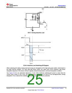
图8-7. Driving Inductive Load
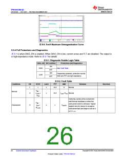
INPUT
VBAT
VOUT
IOUT
VDS, clamp
EHSD
tDECAY
图8-8. Inductive-Load Switching-Off Diagram
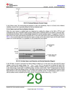
When switching off, battery energy and load energy are dissipated on the high-side power switch, which leads to
the large thermal variation. For each high-side power switch, the upper limit of the maximum safe power
dissipation depends on the device intrinsic capacity, ambient temperature, and board dissipation condition.
See Figure 8-9 for one dedicated inductance, 5 mH. If the maximum switching-off current is lower than the
current value shown on the curve, the internal clamp function can be used for the demagnetization energy
dissipation. If not, external free-wheeling circuitry is necessary for device protection.
Copyright © 2022 Texas Instruments Incorporated
Submit Document Feedback
25
Product Folder Links: TPS1HC100-Q1

 TI [ TEXAS INSTRUMENTS ]