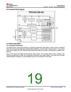
TPS1HC100-Q1
ZHCSLK6A –JULY 2021 –REVISED DECEMBER 2021
www.ti.com.cn
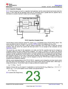
8.3.2.1 Capacitive Charging
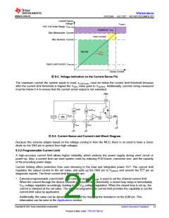
图 8-5 shows the typical set up for a capacitive load application and the internal blocks that function when the
device is used. Note that all capacitive loads have an associated load in parallel with the capacitor that is
described as a resistive load but in reality it can be inductive or resistive.
VBAT
VBB
Smart High Side Switch
EN
Gate Driver
KCL
ILIM1
=
RILIM
ILIM
Current Limiting
Circuit
(VBB – VOUT
RLOAD
)
INOM
=
VOUT
RILIM
CLOAD
GND
RLOAD
ILIM = CLOAD x dVDS/dt
图8-5. Capacitive Charging Circuit
The first thing to check is that the nominal DC current, INOM, is acceptable for the TPS1HC100-Q1 device. This
check can easily be done by taking the RθJA from the Thermal section and multiplying the RON of the
TPS1HC100-Q1 and the INOM with it, add the ambient temperature and if that value is below the thermal
shutdown value the device can operate with that load current. For an example of this calculation see the
Applications section.
The second key care about for this application is to make sure that the capacitive load can be charged up
completely without the device hitting thermal shutdown. The reason is because if the device hits thermal
shutdown during the charging, the resistive nature of the load in parallel with the capacitor starts to discharge the
capacitor over the duration the TPS1HC100-Q1 is off. Note that there are some application with high enough
load impedance that the TPS1HC100-Q1 hitting thermal shutdown and trying again is acceptable; however, for
the majority of applications, the system must be designed so that the TPS1HC100-Q1 does not hit thermal
shutdown while charging the capacitor.
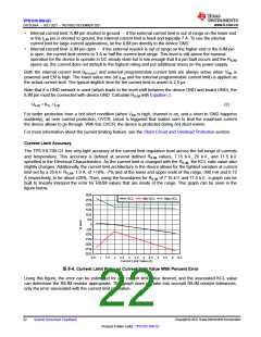
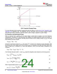
With the current clamping feature of the TPS1HC100-Q1, capacitors can be charged up at a lower inrush current
than other high current limit switches. This lower inrush current means that the capacitor takes a little longer to
charge all the way up. The time that it takes to charge up follows the equation below.
ILIM = C × d(VBB –VDS) / dt
(3)
However, because the VDS for a typical 1 A applications is much less than the VBB voltage (VDS ≈1A × 0.1 Ω=
100 mV, VBB ≈13.5 V), the equation can be rewritten and approximated as
dt = C × dVBB / ILIM
(4)
图8-6 pictures this charge timing.
Copyright © 2022 Texas Instruments Incorporated
Submit Document Feedback
23
Product Folder Links: TPS1HC100-Q1

 TI [ TEXAS INSTRUMENTS ]