TPS1HC100-Q1
ZHCSLK6A –JULY 2021 –REVISED DECEMBER 2021
www.ti.com.cn
Voltage (V)
VBB
VBB - VDS
Time (s)
Current (A)
ICL_ENPS
ICL
INOM
dt
Time (s)
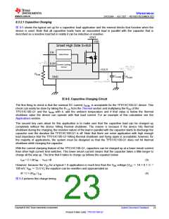
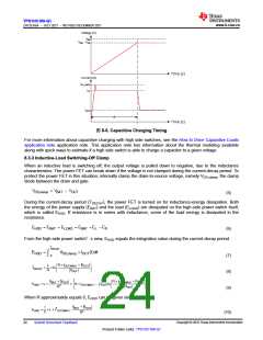
图8-6. Capacitive Charging Timing
For more information about capacitive charging with high side switches, see the How to Drive Capacitive Loads
application note application note. This application note has information about the thermal modeling available
along with quick ways to estimate if a high side switch is able to charge a capacitor to a given voltage.
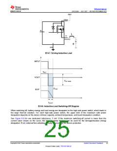
8.3.3 Inductive-Load Switching-Off Clamp
When an inductive load is switching off, the output voltage is pulled down to negative, due to the inductance
characteristics. The power FET can break down if the voltage is not clamped during the current-decay period. To
protect the power FET in this situation, internally clamp the drain-to-source voltage, namely VDS,clamp, the clamp
diode between the drain and gate.
VDS,clamp = VBAT œ VOUT
(5)
During the current-decay period (TDECAY), the power FET is turned on for inductance-energy dissipation. Both
the energy of the power supply (EBAT) and the load (ELOAD) are dissipated on the high-side power switch itself,
which is called EHSD. If resistance is in series with inductance, some of the load energy is dissipated in the
resistance.
EHSD = EBAT + ELOAD = EBAT +EL œ ER
(6)
From the high-side power switch’s view, EHSD equals the integration value during the current-decay period.
TDECAY
EHSD
=
VDS,clamp ì IOUT(t)dt
—
0
(7)
(8)
(9)
≈
’
R ì IOUT(MAX) + VOUT
L
∆
∆
«
÷
÷
◊
TDECAY
=
ì ln
R
VOUT
»
ÿ
Ÿ
VBAT + VOUT
≈ R ì IOUT(MAX) + VOUT
’
…
ì R ì IOUT(MAX) œ VOUT ln
EHSD = L ì
∆
÷
÷
◊
R2
∆
VOUT
…
Ÿ
⁄
«
When R approximately equals 0, EHSD can be given simply as:
VBAT + VOUT
1
2
EHSD
=
ì L ì I2
OUT(MAX)
R2
(10)
Copyright © 2022 Texas Instruments Incorporated
24
Submit Document Feedback
Product Folder Links: TPS1HC100-Q1

 TI [ TEXAS INSTRUMENTS ]