Device Markings
www.ti.com
3
Device Markings
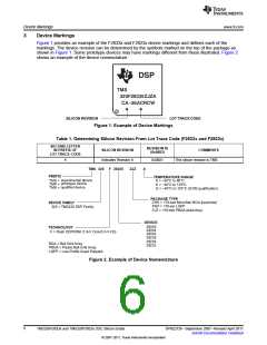
Figure 1 provides an example of the F2833x and F2823x device markings and defines each of the
markings. The device revision can be determined by the symbols marked on the top of the package as
shown in Figure 1. Some prototype devices may have markings different from those illustrated. Figure 2
shows an example of the device nomenclature.
DSP
TMS
320F28335ZJZA
CA−26ACRCW
SILICON REVISION
LOT TRACE CODE
Figure 1. Example of Device Markings
Table 1. Determining Silicon Revision From Lot Trace Code (F2833x and F2823x)
SECOND LETTER
REVISION ID
IN PREFIX OF
SILICON REVISION
COMMENTS
(0x0883)
LOT TRACE CODE
A
Indicates Revision A
0x0001
This silicon revision is TMS.
TMS 320
F
28335
ZJZ
A
PREFIX
TEMPERATURE RANGE
A = −40°C to 85°C
S = −40°C to 125°C
experimental device
prototype device
qualified device
TMX =
TMP =
TMS =
Q = −40°C to 125°C (Q100 qualification)
PACKAGE TYPE
ZHH = 179-ball MicroStar BGA (lead-free)
PGF = 176-pin LQFP
ZJZ = 176-ball PBGA (lead-free)
DEVICE FAMILY
320 = TMS320 DSP Family
DEVICE
28335
28334
28332
28235
28234
28232
TECHNOLOGY
F = Flash EEPROM (1.9-V Core/3.3-V I/O)
BGA = Ball Grid Array
PBGA = Plastic Ball Grid Array
LQFP = Low-Profile Quad Flatpack
Figure 2. Example of Device Nomenclature
6
TMS320F2833x and TMS320F2823x DSC Silicon Errata
SPRZ272F–September 2007–Revised April 2011
Submit Documentation Feedback
© 2007–2011, Texas Instruments Incorporated

 TI [ TEXAS INSTRUMENTS ]