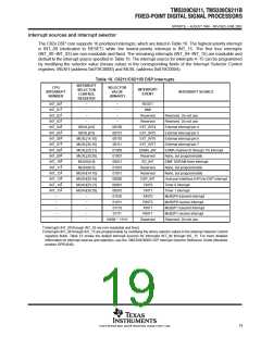
ꢀ ꢁꢂ ꢃ ꢄ ꢅ ꢆꢇ ꢄ ꢈꢈ ꢉ ꢀ ꢁꢂ ꢃ ꢄꢅ ꢆꢇ ꢄꢈꢈꢊ
ꢋ ꢌꢍ ꢎꢏꢐꢑꢒ ꢌ ꢓꢀ ꢏꢌ ꢔꢌ ꢀꢕꢖ ꢂꢌ ꢔ ꢓꢕꢖ ꢑꢗ ꢒ ꢆꢎ ꢂ ꢂꢒ ꢗ ꢂ
SPRS073L − AUGUST 1998 − REVISED JUNE 2005
§
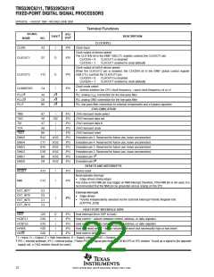
PLLV and PLLG are not part of external voltage supply or ground. See the CLOCK/PLL documentation for information on how to connect these
pins.
¶
#
A = Analog signal (PLL Filter)
The EMU0 and EMU1 pins are internally pulled up with 30-kΩ resistors; therefore, for emulation and normal operation, no external
pullup/pulldown resistors are necessary. However, for boundary scan operation, pull down the EMU1 and EMU0 pins with a dedicated 1-kΩ
resistor.
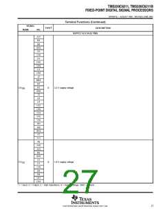
Terminal Functions (Continued)
SIGNAL
NAME
IPD/
IPU‡
†
TYPE
DESCRIPTION
HOST-PORT INTERFACE (HPI) (CONTINUED)
NO.
HD15
B14
C14
A15
C15
A16
B16
C16
B17
A18
C17
B18
C19
C20
D18
D20
E20
E18
F20
E19
F18
H19
IPU
IPU
IPU
IPU
IPU
IPU
IPU
IPU
IPU
IPU
IPU
IPD
IPU
IPU
IPU
IPU
IPU
IPU
IPU
IPU
IPD
HD14
HD13
HD12
HD11
HD10
HD9
Host-port data
•
•
Used for transfer of data, address, and control
Also controls initialization of DSP modes at reset via pullup/pulldown resistors
− Device Endian mode
HD8: 0 – Big Endian
HD8
I/O/Z
1 − Little Endian
HD7
− Boot mode
HD[4:3]: 00 – HPI boot
01 − 8-bit ROM boot with default timings
HD6
HD5
10 − 16-bit ROM boot with default timings
11 − 32-bit ROM boot with default timings
HD4
HD3
HD2
HD1
HD0
HAS
HCS
HDS1
HDS2
HRDY
I
I
Host address strobe
Host chip select
I
Host data strobe 1
I
Host data strobe 2
O
Host ready (from DSP to host)
EMIF − CONTROL SIGNALS COMMON TO ALL TYPES OF MEMORY
CE3
CE2
CE1
CE0
BE3
BE2
BE1
BE0
V6
W6
W18
V17
V5
O/Z
O/Z
O/Z
O/Z
O/Z
O/Z
O/Z
O/Z
IPU
Memory space enables
IPU
•
•
Enabled by bits 28 through 31 of the word address
Only one asserted during any external data access
IPU
IPU
IPU
IPU
IPU
IPU
Byte-enable control
Y4
•
•
•
Decoded from the two lowest bits of the internal address
Byte-write enables for most types of memory
Can be directly connected to SDRAM read and write mask signal (SDQM)
U19
V20
†
‡
I = Input, O = Output, Z = High impedance, S = Supply voltage, GND = Ground
IPD = Internal pulldown, IPU = Internal pullup. (These IPD/IPU signal pins feature a 30-kΩ IPD or IPU resistor. To pull up a signal to the opposite
supply rail, a 1-kΩ resistor should be used.)
23
POST OFFICE BOX 1443 • HOUSTON, TEXAS 77251−1443

 TI [ TEXAS INSTRUMENTS ]