ꢀ ꢁ ꢂ ꢃ ꢄꢅ ꢆ ꢇ ꢄꢈꢈ ꢉ ꢀꢁ ꢂꢃ ꢄ ꢅ ꢆꢇ ꢄ ꢈꢈ ꢊ
ꢋ ꢌ ꢍꢎꢏ ꢐꢑ ꢒꢌ ꢓ ꢀ ꢏ ꢌ ꢔꢌ ꢀꢕꢖ ꢂ ꢌ ꢔꢓ ꢕꢖ ꢑ ꢗꢒ ꢆꢎꢂ ꢂꢒ ꢗꢂ
SPRS073L − AUGUST 1998 − REVISED JUNE 2005
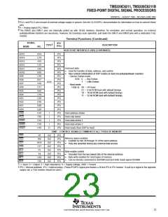
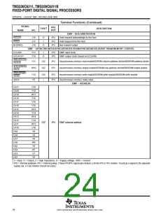
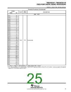
Terminal Functions
SIGNAL
NAME
IPD/
IPU
†
DESCRIPTION
TYPE
‡
NO.
A3
CLOCK/PLL
CLKIN
I
IPD
IPD
Clock Input
Clock output at device speed
The CLK1EN bit in the EMIF GBLCTL register controls the CLKOUT1 pin.
CLKOUT1
D7
O
CLK1EN = 0:
CLK1EN = 1:
CLKOUT1 is disabled
CLKOUT1 enabled to clock [default]
Clock output at half of device speed
When the CLKOUT2 pin is enabled, the CLK2EN bit in the EMIF global control register
(GBLCTL) controls the CLKOUT2 pin.
CLKOUT2
Y12
C4
O
I
IPD
IPU
CLK2EN = 0:
CLK2EN = 1:
CLKOUT2 is disabled
CLKOUT1 enabled to clock [default]
Clock mode select
CLKMODE0
•
Selects whether the CPU clock frequency = input clock frequency x4 or x1
§
¶
A
¶
A
¶
A
PLLV
A4
C6
B5
PLL analog V
connection for the low-pass filter
CC
§
PLLG
PLL analog GND connection for the low-pass filter
PLL low-pass filter connection to external components and a bypass capacitor
JTAG EMULATION
PLLF
TMS
TDO
TDI
B7
A8
I
IPU
IPU
IPU
IPU
IPD
IPU
IPU
IPU
IPU
IPU
IPU
JTAG test-port mode select
O/Z
JTAG test-port data out
A7
I
I
I
JTAG test-port data in
TCK
A6
JTAG test-port clock
TRST
EMU5
EMU4
EMU3
EMU2
EMU1
EMU0
B6
JTAG test-port reset
B12
C11
B10
D10
B9
I/O/Z
I/O/Z
I/O/Z
I/O/Z
I/O/Z
I/O/Z
Emulation pin 5. Reserved for future use, leave unconnected.
Emulation pin 4. Reserved for future use, leave unconnected.
Emulation pin 3. Reserved for future use, leave unconnected.
Emulation pin 2. Reserved for future use, leave unconnected.
#
Emulation pin 1
Emulation pin 0
#
D9
RESETS AND INTERRUPTS
Device reset
Nonmaskable interrupt
Edge-driven (rising edge)
Any noise on the NMI pin may trigger an NMI interrupt; therefore, if the NMI pin is not used, it is
recommended that the NMI pin be grounded versus relying on the IPD.
RESET
NMI
A13
C13
I
I
IPU
IPD
•
EXT_INT7
EXT_INT6
EXT_INT5
EXT_INT4
E3
D2
C1
C2
External interrupts
•
•
Edge-driven
I
IPU
Polarity independently selected via the External Interrupt Polarity Register bits
(EXTPOL.[3:0])
HOST-PORT INTERFACE (HPI)
HINT
J20
G19
G18
H20
G20
O
I
IPU
IPU
IPU
IPU
IPU
Host interrupt (from DSP to host)
HCNTL1
HCNTL0
HHWIL
HR/W
Host control − selects between control, address, or data registers
Host control − selects between control, address, or data registers
Host half-word select − first or second half-word (not necessarily high or low order)
Host read or write select
I
I
I
†
‡
I = Input, O = Output, Z = High impedance, S = Supply voltage, GND = Ground
IPD = Internal pulldown, IPU = Internal pullup. (These IPD/IPU signal pins feature a 30-kΩ IPD or IPU resistor. To pull up a signal to the opposite
supply rail, a 1-kΩ resistor should be used.)
22
POST OFFICE BOX 1443 • HOUSTON, TEXAS 77251−1443

 TI [ TEXAS INSTRUMENTS ]