Electrical Specifications
6.3
Electrical Characteristics Over Recommended Operating Conditions
(Unless Otherwise Noted)
PARAMETER
TEST CONDITIONS
MIN
TYP
MAX
UNIT
V
I
= I
MAX
= 50 µA
2.4
OH OH
V
V
High-level output voltage
Low-level output voltage
OH
I
I
V
− 0.2
OH
DDIO
= I MAX
OL OL
0.4
V
OL
Input
current
(low level)
With pullup
V
= 3.3 V, V = 0 V
IN
−80
−140 −190
DDIO
DDIO
†
I
IL
µA
With pulldown
V
= 3.3 V, V = 0 V
IN
±2
§
All I/Os (including XRS)
−80
−13
−140 −190
V
V
= 3.3 V,
= 0 V
Input
current
(low level)
DDIO
IN
except EVB
With pullup
‡
I
µA
IL
GPIOB/EVB
−25
−35
With pulldown
With pullup
V
V
= 3.3 V, V = 0 V
IN
±2
DDIO
DDIO
DDIO
= 3.3 V, V = V
IN
±2
DD
Input
current
(high level)
I
I
µA
µA
IH
V
V
= 3.3 V,
DD
¶
With pulldown
28
50
80
= V
IN
Output current,
high-impedance state
(off-state)
V
O
= V
DDIO
or 0 V
±2
OZ
C
C
Input capacitance
Output capacitance
2
3
pF
pF
i
o
†
‡
§
¶
Applicable to C281x devices
Applicable to F281x devices
The following pins have no internal PU/PD: GPIOE0, GPIOE1, GPIOF0, GPIOF1, GPIOF2, GPIOF3, GPIOF12, GPIOG4, and GPIOG5.
The following pins have an internal pulldown: XMP/MC, TESTSEL, and TRST.
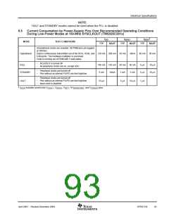
6.4
Current Consumption by Power-Supply Pins Over Recommended Operating Conditions
During Low-Power Modes at 150-MHz SYSCLKOUT (TMS320F281x)
†
I
I
I
I
DDA
DD
DDIO
DD3VFL
MODE
TEST CONDITIONS
‡
MAX
‡
MAX
‡
MAX
‡
MAX
TYP
TYP
TYP
TYP
All peripheral clocks are enabled. All
PWM pins are toggled at 100 kHz.
Data is continuously transmitted out of
the SCIA, SCIB, and CAN ports. The
hardware multiplier is exercised.
Code is running out of flash with 5
wait-states.
Operational
195 mA 230 mA
15 mA
30 mA
40 mA
45 mA
40 mA
50 mA
−
−
−
Flash is powered down
XCLKOUT is turned off
All peripheral clocks are on,
except ADC
IDLE
125 mA 150 mA
5 mA
10 mA
2 µA
2 µA
4 µA
4 µA
1 µA
1 µA
20 µA
20 µA
−
−
−
Flash is powered down
Peripheral clocks are turned off
Pins without an internal PU/PD
are tied high/low
STANDBY
5 mA
10 mA
5 µA
20 µA
−
−
−
Flash is powered down
Peripheral clocks are turned off
Pins without an internal PU/PD
are tied high/low
HALT
70 µA
5 µA
20 µA
2 µA
4 µA
1 µA
20 µA
−
Input clock is disabled
†
‡
I
includes current into V
, V
, V
, AV
DDREFBG
, and V
DDAIO
pins.
DDA
DDA1 DDA2 DD1
MAX numbers are at 125°C, and MAX voltage (V
DD
= 2.0 V; V = 3.6 V).
, V
, V
DDIO DD3VFL DDA
92
SPRS174L
April 2001 − Revised December 2004

 TI [ TEXAS INSTRUMENTS ]