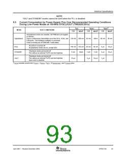
Electrical Specifications
6
Electrical Specifications
This section provides the absolute maximum ratings and the recommended operating conditions for the
TMS320F281x and TMS320C281x DSPs.
6.1
Absolute Maximum Ratings
Unless otherwise noted, the list of absolute maximum ratings are specified over operating temperature
ranges. Stresses beyond those listed under Absolute Maximum Ratings may cause permanent damage to
the device. These are stress ratings only, and functional operation of the device at these or any other
conditions beyond those indicated under Section 6.2 is not implied. Exposure to absolute-maximum-rated
conditions for extended periods may affect device reliability. All voltage values are with respect to V
.
SS
Supply voltage range, V
, V
, V
, V
, and AV
. . . . . . . . . . . . . − 0.3 V to 4.6 V
DDIO DDA1 DDA2 DDAIO
DDREFBG
Supply voltage range, V , V
. . . . . . . . . . . . . . . . . . . . . . . . . . . . . . . . . . . . . . . . . . . . . . . . − 0.5 V to 2.5 V
DD DD1
V
range . . . . . . . . . . . . . . . . . . . . . . . . . . . . . . . . . . . . . . . . . . . . . . . . . . . . . . . . . . . . . . . . − 0.3 V to 4.6 V
DD3VFL
Input voltage range, V
. . . . . . . . . . . . . . . . . . . . . . . . . . . . . . . . . . . . . . . . . . . . . . . . . . . . . . . . . − 0.3 V to 4.6 V
IN
Output voltage range, V
. . . . . . . . . . . . . . . . . . . . . . . . . . . . . . . . . . . . . . . . . . . . . . . . . . . . . . . − 0.3 V to 4.6 V
†
O
Input clamp current, I (V < 0 or V > V
DDIO
)
. . . . . . . . . . . . . . . . . . . . . . . . . . . . . . . . . . . . . . . . . ± 20 mA
IK IN
IN
Output clamp current, I
(V < 0 or V > V
) . . . . . . . . . . . . . . . . . . . . . . . . . . . . . . . . . . . . . . . . ± 20 mA
OK
O
O
DDIO
‡
Operating ambient temperature ranges, T : A version (GHH, PGF, PBK) . . . . . . . . . . . . . . − 40°C to 85°C
A
‡§
T : S version (GHH, PGF, PBK)
. . . . . . . . . . . . − 40°C to 125°C
A
‡
T : Q version (GHH, PGF, PBK) . . . . . . . . . . . . . − 40°C to 125°C
A
†
Storage temperature range, T
. . . . . . . . . . . . . . . . . . . . . . . . . . . . . . . . . . . . . . . . . . . . . . . . − 65°C to 150°C
stg
†
Continuous clamp current per pin is± 2 mA
‡
Long-term high-temperature storage and/or extended use at maximum temperature conditions may result in a reduction of overall device life.
For additional information, see IC Package Thermal Metrics Application Report (literature number SPRA953) and Reliability Data for
TMS320LF24x and TMS320F281x Devices Application Report (literature number SPRA963).
§
Replaced by Q temperature option from silicon revision E onwards
90
SPRS174L
April 2001 − Revised December 2004

 TI [ TEXAS INSTRUMENTS ]