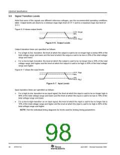
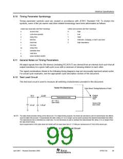
Electrical Specifications
6.7
Reducing Current Consumption
28x DSPs incorporate a unique method to reduce the device current consumption. A reduction in current
consumption can be achieved by turning off the clock to any peripheral module which is not used in a given
application. Table 6−1 indicates the typical reduction in current consumption achieved by turning off the clocks
to various peripherals.
†
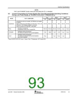
Table 6−1. Typical Current Consumption by Various Peripherals (at 150 MHz)
PERIPHERAL MODULE
I
CURRENT REDUCTION (mA)
DD
12
6
eCAN
EVA
6
EVB
‡
8
ADC
SCI
4
SPI
5
McBSP
13
†
‡
All peripheral clocks are disabled upon reset. Writing to/reading from peripheral registers is possible only after the peripheral clocks are turned
on.
This number represents the current drawn by the digital portion of the ADC module. Turning off the clock to the ADC module results in the
elimination of the current drawn by the analog portion of the ADC (I
) as well.
CCA
6.8
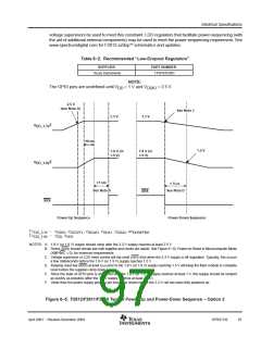
Power Sequencing Requirements
TMS320F2812/F2811/F2810 silicon requires dual voltages (1.8-V or 1.9-V and 3.3-V) to power up the CPU,
Flash, ROM, ADC, and the I/Os. To ensure the correct reset state for all modules during power up, there are
some requirements to be met while powering up/powering down the device. The current F2812 silicon
reference schematics (Spectrum Digital Incorporated eZdsp. board) suggests two options for the power
sequencing circuit.
Power sequencing is not needed for C281x devices. In other words, 3.3-V and 1.8-V (or 1.9-V) can ramp
together. C281x can also be used on boards that have F281x power sequencing implemented; however, if
the 1.8-V (or 1.9-V) rail lags the 3.3-V rail, the GPIO pins are undefined until the 1.8-V rail reaches at least
1 V.
•
Option 1:
In this approach, an external power sequencing circuit enables V
first, then V
and V
(1.8 V or
DDIO
DD
DD1
1.9 V). After 1.8 V (or 1.9 V) ramps, the 3.3 V for Flash (V
) and ADC (V
/V
/AV
)
DD3VFL
DDA1 DDA2
DDREFBG
modules are ramped up. While option 1 is still valid, TI has simplified the requirement. Option 2 is the
recommended approach.
•
Option 2:
Enable power to all 3.3-V supply pins (V
, V
, V
/V
/V
/AV
) and then
DDIO DD3VFL DDA1 DDA2 DDAIO
DDREFBG
ramp 1.8 V (or 1.9 V) (V /V
) supply pins.
DD DD1
1.8 V or 1.9 V (V /V
) should not reach 0.3 V until V
has reached 2.5 V. This ensures the reset
DD DD1
DDIO
signal from the I/O pin has propagated through the I/O buffer to provide power-on reset to all the modules
inside the device. See Figure 6−10 for power-on reset timing.
•
Power-Down Sequencing:
During power-down, the device reset should be asserted low (8 µs, minimum) before the V
supply
power supplies
DD
reaches 1.5 V. This will help to keep on-chip flash logic in reset prior to the V
/V
DDIO DD
ramping down. It is recommended that the device reset control from “Low-Dropout (LDO)” regulators or
eZdsp is a trademark of Spectrum Digital Incorporated.
96
SPRS174L
April 2001 − Revised December 2004

 TI [ TEXAS INSTRUMENTS ]