TMS320F28027, TMS320F28027-Q1, TMS320F28027F, TMS320F28027F-Q1, TMS320F28026
TMS320F28026-Q1, TMS320F28026F, TMS320F28026F-Q1, TMS320F28023
TMS320F28023-Q1, TMS320F28022, TMS320F28021, TMS320F28020, TMS320F280200
ZHCSA13P –NOVEMBER 2008 –REVISED FEBRUARY 2021
www.ti.com.cn
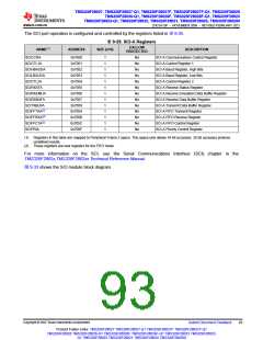
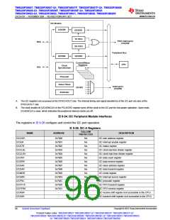
The SCI port operation is configured and controlled by the registers listed in 表9-25.
表9-25. SCI-A Registers
EALLOW
PROTECTED
NAME(1)
SCICCRA
ADDRESS
SIZE (x16)
DESCRIPTION
0x7050
0x7051
0x7052
0x7053
0x7054
0x7055
0x7056
0x7057
0x7059
0x705A
0x705B
0x705C
0x705F
1
1
1
1
1
1
1
1
1
1
1
1
1
No
No
No
No
No
No
No
No
No
No
No
No
No
SCI-A Communications Control Register
SCI-A Control Register 1
SCICTL1A
SCIHBAUDA
SCILBAUDA
SCICTL2A
SCI-A Baud Register, High Bits
SCI-A Baud Register, Low Bits
SCI-A Control Register 2
SCIRXSTA
SCIRXEMUA
SCIRXBUFA
SCITXBUFA
SCIFFTXA(2)
SCIFFRXA(2)
SCIFFCTA(2)
SCIPRIA
SCI-A Receive Status Register
SCI-A Receive Emulation Data Buffer Register
SCI-A Receive Data Buffer Register
SCI-A Transmit Data Buffer Register
SCI-A FIFO Transmit Register
SCI-A FIFO Receive Register
SCI-A FIFO Control Register
SCI-A Priority Control Register
(1) Registers in this table are mapped to Peripheral Frame 2 space. This space only allows 16-bit accesses. 32-bit accesses produce
undefined results.
(2) These registers are new registers for the FIFO mode.
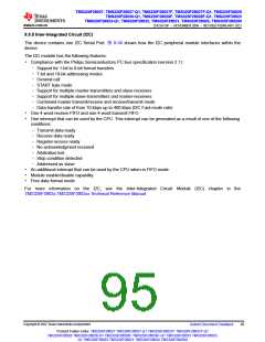
For more information on the SCI, see the Serial Communications Interface (SCI) chapter in the
TMS320F2802x,TMS320F2802xx Technical Reference Manual.
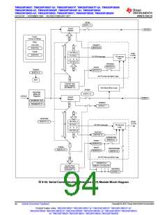
图9-33 shows the SCI module block diagram.
Copyright © 2022 Texas Instruments Incorporated
Submit Document Feedback
93
Product Folder Links: TMS320F28027 TMS320F28027-Q1 TMS320F28027F TMS320F28027F-Q1
TMS320F28026 TMS320F28026-Q1 TMS320F28026F TMS320F28026F-Q1 TMS320F28023 TMS320F28023-
Q1 TMS320F28022 TMS320F28021 TMS320F28020 TMS320F280200

 TI [ TEXAS INSTRUMENTS ]