TMS320F28027, TMS320F28027-Q1, TMS320F28027F, TMS320F28027F-Q1, TMS320F28026
TMS320F28026-Q1, TMS320F28026F, TMS320F28026F-Q1, TMS320F28023
TMS320F28023-Q1, TMS320F28022, TMS320F28021, TMS320F28020, TMS320F280200
ZHCSA13P –NOVEMBER 2008 –REVISED FEBRUARY 2021
www.ti.com.cn
9.9 外设
9.9.1 Analog Block
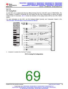
A 12-bit ADC core is implemented that has different timings than the 12-bit ADC used on F280x/F2833x. The
ADC wrapper is modified to incorporate the new timings and also other enhancements to improve the timing
control of start of conversions. 图 9-16 shows the interaction of the analog module with the rest of the F2802x
system.
For more information on the ADC, see the Analog-to-Digital Converter and Comparator chapter in the
TMS320F2802x,TMS320F2802xx Technical Reference Manual.
(3.3 V) VDDA
(Agnd) VSSA
VREFLO
38-Pin
VDDA
48-Pin
VDDA
VREFLO VREFLO
Tied To Tied To
Interface Reference
Diff
VSSA
VSSA
VREFHI VREFHI
Tied To Tied To
VREFHI
A0
B0
A0
A2
A4
A6
A0
A1
A2
A3
A4
A1
B1
COMP1OUT
A2
AIO2
AIO10
10-Bit
DAC
Comp1
Comp2
B2
A6
A7
A3
B3
ADC
COMP2OUT
(See Note A)
A4
B4
B1
B2
B3
B4
AIO4
AIO12
10-Bit
DAC
B2
B4
B6
B5
B6
B7
Temperature Sensor
A5
A6
Signal Pinout
AIO6
AIO14
B6
A7
B7
A. Comparator 2 is available only on the 48-pin PT package.
图9-16. Analog Pin Configurations
Copyright © 2022 Texas Instruments Incorporated
Submit Document Feedback
69
Product Folder Links: TMS320F28027 TMS320F28027-Q1 TMS320F28027F TMS320F28027F-Q1
TMS320F28026 TMS320F28026-Q1 TMS320F28026F TMS320F28026F-Q1 TMS320F28023 TMS320F28023-
Q1 TMS320F28022 TMS320F28021 TMS320F28020 TMS320F280200

 TI [ TEXAS INSTRUMENTS ]