TMS320F28027, TMS320F28027-Q1, TMS320F28027F, TMS320F28027F-Q1, TMS320F28026
TMS320F28026-Q1, TMS320F28026F, TMS320F28026F-Q1, TMS320F28023
TMS320F28023-Q1, TMS320F28022, TMS320F28021, TMS320F28020, TMS320F280200
ZHCSA13P –NOVEMBER 2008 –REVISED FEBRUARY 2021
www.ti.com.cn
9.8.1 External Interrupts
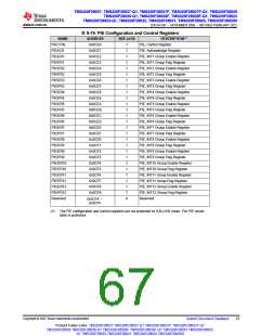
表9-20. External Interrupt Registers
NAME
XINT1CR
XINT2CR
XINT3CR
XINT1CTR
XINT2CTR
XINT3CTR
ADDRESS
0x00 7070
0x00 7071
0x00 7072
0x00 7078
0x00 7079
0x00 707A
SIZE (x16)
DESCRIPTION
XINT1 configuration register
XINT2 configuration register
XINT3 configuration register
XINT1 counter register
1
1
1
1
1
1
XINT2 counter register
XINT3 counter register
Each external interrupt can be enabled/disabled or qualified using positive, negative, or both positive and
negative edge. For more information, see the System Control chapter in the TMS320F2802x,TMS320F2802xx
Technical Reference Manual.
9.8.1.1 外部中断电子数据/定时
9.8.1.1.1 External Interrupt Timing Requirements
MIN(1)
1tc(SCO)
MAX
UNIT
cycles
cycles
Synchronous
With qualifier
(2)
tw(INT)
Pulse duration, INT input low/high
1tc(SCO) + tw(IQSW)
(1) For an explanation of the input qualifier parameters, see 节9.9.10.1.2.1.
(2) This timing is applicable to any GPIO pin configured for ADCSOC functionality.
9.8.1.1.2 External Interrupt Switching Characteristics
over recommended operating conditions (unless otherwise noted)
PARAMETER
MIN(1)
MAX
tw(IQSW) + 12tc(SCO)
UNIT
td(INT)
Delay time, INT low/high to interrupt-vector fetch
cycles
(1) For an explanation of the input qualifier parameters, see 节9.9.10.1.2.1.
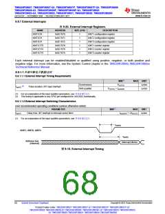
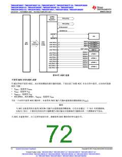
t
w(INT)
XINT1, XINT2, XINT3
t
d(INT)
Address bus
(internal)
Interrupt Vector
图9-15. External Interrupt Timing
Copyright © 2022 Texas Instruments Incorporated
68
Submit Document Feedback
Product Folder Links: TMS320F28027 TMS320F28027-Q1 TMS320F28027F TMS320F28027F-Q1
TMS320F28026 TMS320F28026-Q1 TMS320F28026F TMS320F28026F-Q1 TMS320F28023 TMS320F28023-
Q1 TMS320F28022 TMS320F28021 TMS320F28020 TMS320F280200

 TI [ TEXAS INSTRUMENTS ]