TMS320F28027, TMS320F28027-Q1, TMS320F28027F, TMS320F28027F-Q1, TMS320F28026
TMS320F28026-Q1, TMS320F28026F, TMS320F28026F-Q1, TMS320F28023
TMS320F28023-Q1, TMS320F28022, TMS320F28021, TMS320F28020, TMS320F280200
ZHCSA13P –NOVEMBER 2008 –REVISED FEBRUARY 2021
www.ti.com.cn
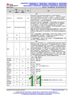
8 规格
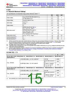
8.1 Absolute Maximum Ratings
over operating free-air temperature range (unless otherwise noted)(1) (2)
MIN
–0.3
–0.3
–0.3
–0.3
–0.3
–0.3
MAX
4.6
2.5
4.6
4.6
2.5
4.6
UNIT
VDDIO (I/O and Flash) with respect to VSS
Supply voltage
V
V
V
V
VDD with respect to VSS
Analog voltage
Input voltage
Output voltage
VDDA with respect to VSSA
VIN (3.3 V)
VIN (X1)
VO
Digital/analog input (per pin), IIK
20
20
20
–20
–20
–20
(3)
(VIN < VSS or VIN > VDDIO
)
Analog input (per pin), IIKANALOG
(VIN < VSSA or VIN > VDDA
Input clamp current
mA
)
Total for all inputs, IIKTOTAL
(VIN < VSS/VSSA or VIN > VDDIO/VDDA
)
Output clamp current
Junction temperature(4)
Storage temperature(4)
IOK (VO < 0 or VO > VDDIO
)
20
150
150
mA
°C
–20
–40
–65
TJ
Tstg
°C
(1) Stresses beyond those listed under Absolute Maximum Ratings may cause permanent damage to the device. These are stress ratings
only, and functional operation of the device at these or any other conditions beyond those indicated under 节8.4 is not implied.
Exposure to absolute-maximum-rated conditions for extended periods may affect device reliability.
(2) All voltage values are with respect to VSS, unless otherwise noted.
(3) Continuous clamp current per pin is ±2 mA. Do not operate in this condition continuously as VDDIO/VDDA voltage may internally rise and
impact other electrical specifications.
(4) Long-term high-temperature storage or extended use at maximum temperature conditions may result in a reduction of overall device
life. For additional information, see Semiconductor and IC Package Thermal Metrics; Calculating Useful Lifetimes of Embedded
Processors; and Calculating FIT for a Mission Profile.
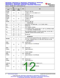
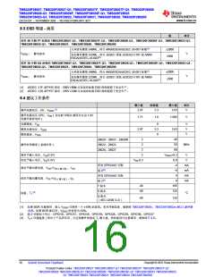
8.2 ESD 等级- 汽车
值
单位
采用48 引脚PT 封装的TMS320F28027-Q1、TMS320F28027F-Q1、TMS320F28026-Q1、TMS320F28026F-Q1、TMS320F28023-Q1、
TMS320F28022-Q
人体放电模型(HBM),符合AEC Q100-002(1)
±2000
所有引脚
除边角引脚以外的所有引
脚
±500
V(ESD)
V
静电放电
充电器件模型(CDM),符合AEC Q100-011
48 引脚PT 上的转角引
脚:1、12、13、24、
25、36、37、48
±750
采用38 引脚DA 封装的TMS320F28027-Q1、TMS320F28027F-Q1、TMS320F28026-Q1、TMS320F28026F-Q1、TMS320F28023-Q1、
TMS320F28022-Q1
人体放电模型(HBM),符合AEC Q100-002(1)
±2000
所有引脚
除边角引脚以外的所有引
脚
±500
V(ESD)
V
静电放电
充电器件模型(CDM),符合AEC Q100-011
38 引脚DA 上的转角引
脚:1、19、20、38
±750
(1) AEC Q100-002 指示应当按照ANSI/ESDA/JEDEC JS-001 规范执行HBM 应力测试。
Copyright © 2022 Texas Instruments Incorporated
Submit Document Feedback
15
Product Folder Links: TMS320F28027 TMS320F28027-Q1 TMS320F28027F TMS320F28027F-Q1
TMS320F28026 TMS320F28026-Q1 TMS320F28026F TMS320F28026F-Q1 TMS320F28023 TMS320F28023-
Q1 TMS320F28022 TMS320F28021 TMS320F28020 TMS320F280200

 TI [ TEXAS INSTRUMENTS ]