TMS320DM6437
Digital Media Processor
www.ti.com
SPRS345B–NOVEMBER 2006–REVISED MARCH 2007
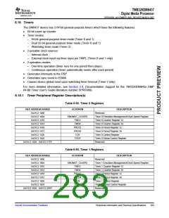
Table 6-94. Timer 2 (Watchdog) Registers
HEX ADDRESS RANGE
0x01C2 1C00
ACRONYM
DESCRIPTION
-
EMUMGT_CLKSPD
TIM12
Reserved
0x01C2 1C04
Timer 2 Emulation Management/Clock Speed Register
Timer 2 Counter Register 12
Timer 2 Counter Register 34
Timer 2 Period Register 12
0x01C2 1C10
0x01C2 1C14
TIM34
0x01C2 1C18
PRD12
PRD34
TCR
0x01C2 1C1C
Timer 2 Period Register 34
0x01C2 1C20
Timer 2 Control Register
0x01C2 1C24
TGCR
Timer 2 Global Control Register
Timer 2 Watchdog Timer Control Register
Reserved
0x01C2 1C28
WDTCR
-
0x01C2 1C2C - 0x01C2 1FFF
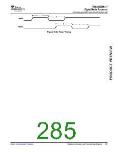
6.19.2 Timer Electrical Data/Timing
Table 6-95. Timing Requirements for Timer Input(1)(2)(3) (see Figure 6-52)
-400
-500
-600
NO.
UNIT
MIN
MAX
TINP0L, if TIMERCTL.TINP0SEL = 0
[default]
2P
ns
1
tw(TINPH)
Pulse duration, TINPxL high
TINP0L, if TIMERCTL.TINP0SEL = 1
0.33P
2P
ns
ns
TINP1L
TINP0L, if TIMERCTL.TINP0SEL = 0
[default]
2P
ns
2
tw(TINPL)
Pulse duration, TINPxL low
TINP0L, if TIMERCTL.TINP0SEL = 1
0.33P
2P
ns
ns
TINP1L
(1) P = MXI/CLKIN cycle time in ns. For example, when MXI/CLKIN frequency is 27 MHz, use P = 37.037 ns.
(2) The TIMERCTL.TINP0SEL field in the System Module determines if the TINP0L input directly goes to Timer 0
(TIMERCTL.TINP0SEL=0), or if the TINP0L input is first divided down by 6 before going to Timer 0 (TIMERCTL.TINP0SEL=1).
(3) TINP1L input goes directly to Timer 1.
Table 6-96. Switching Characteristics Over Recommended Operating Conditions for Timer Output(1) (see
Figure 6-52)
-400
-500
-600
NO.
UNIT
MIN
MAX
3
4
tw(TOUTH)
tw(TOUTL)
Pulse duration, TOUTxL high
Pulse duration, TOUTxL low
P
P
ns
ns
(1) P = MXI/CLKIN cycle time in ns. For example, when MXI/CLKIN frequency is 27 MHz, use P = 37.037 ns.
284
Peripheral Information and Electrical Specifications
Submit Documentation Feedback

 TI [ TEXAS INSTRUMENTS ]