TMS320DM6437
Digital Media Processor
www.ti.com
SPRS345B–NOVEMBER 2006–REVISED MARCH 2007
6.20.2 PCI Peripheral Register Description(s)
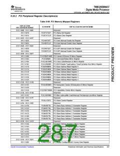
Table 6-98. PCI Memory-Mapped Registers
DSP ACCESS
HEX ADDRESS RANGE
ACRONYM
DSP ACCESS REGISTER NAME
01C1 A000 - 01C1 A00F
01C1 A010
-
Reserved
PCISTATSET
PCISTATCLR
-
PCI Status Set Register
01C1 A014
PCI Status Clear Register
Reserved
01C1 A018 - 01C1 A01F
01C1 A020
PCIHINTSET
PCIHINTCLR
-
PCI Host Interrupt Enable Set Register
PCI Host Interrupt Enable Clear Register
Reserved
01C1 A024
01C1 A028 - 01C1 A02F
01C1 A030
PCIDINTSET
PCIDINTCLR
-
PCI DSP Interrupt Enable Set Register
PCI DSP Interrupt Enable Clear Register
Reserved
01C1 A034
01C1 A038 - 01C1 A0FF
01C1 A100
PCIVENDEVMIR PCI Vendor ID/Device ID Mirror Register
PCICSRMIR PCI Command/Status Mirror Register
PCICLREVMIR PCI Class Code/Revision ID Mirror Register
01C1 A104
01C1 A108
01C1 A10C
PCICLINEMIR
PCIBAR0MSK
PCIBAR1MSK
PCIBAR2MSK
PCIBAR3MSK
PCIBAR4MSK
PCIBAR5MSK
-
PCI BIST/Header Type/Latency Timer/Cacheline Size Mirror Register
01C1 A110
PCI Base Address Mask Register 0
PCI Base Address Mask Register 1
PCI Base Address Mask Register 2
PCI Base Address Mask Register 3
PCI Base Address Mask Register 4
PCI Base Address Mask Register 5
Reserved
01C1 A114
01C1 A118
01C1 A11C
01C1 A120
01C1 A124
01C1 A128 - 01C1 A12B
01C1 A12C
PCISUBIDMIR
-
PCI Subsystem Vendor ID/Subsystem ID Mirror Register
Reserved
01C1 A130
01C1 A134
PCICPBPTRMIR PCI Capabilities Pointer Mirror Register
01C1 A138 - 01C1 A13B
01C1 A13C
-
Reserved
PCILGINTMIR
-
PCI Max Latency/Min Grant/Interrupt Pin/Interrupt Line Mirror Register
Reserved
01C1 A140 - 01C1 A17F
01C1 A180
PCISLVCNTL
-
PCI Slave Control Register
01C1 A184 - 01C1 A1BF
01C1 A1C0
Reserved
PCIBAR0TRL
PCIBAR1TRL
PCIBAR2TRL
PCIBAR3TRL
PCIBAR4TRL
PCIBAR5TRL
-
PCI Slave Base Address 0 Translation Register
PCI Slave Base Address 1 Translation Register
PCI Slave Base Address 2 Translation Register
PCI Slave Base Address 3 Translation Register
PCI Slave Base Address 4 Translation Register
PCI Slave Base Address 5 Translation Register
Reserved
01C1 A1C4
01C1 A1C8
01C1 A1CC
01C1 A1D0
01C1 A1D4
01C1 A1D8 - 01C1 A1DF
01C1 A1E0
PCIBAR0MIR
PCIBAR1MIR
PCIBAR2MIR
PCIBAR3MIR
PCIBAR4MIR
PCIBAR5MIR
-
PCI Base Address Register 0 Mirror Register
PCI Base Address Register 1 Mirror Register
PCI Base Address Register 2 Mirror Register
PCI Base Address Register 3 Mirror Register
PCI Base Address Register 4 Mirror Register
PCI Base Address Register 5 Mirror Register
Reserved
01C1 A1E4
01C1 A1E8
01C1 A1EC
01C1 A1F0
01C1 A1F4
01C1 A1F8 - 01C1 A2FF
01C1 A300
PCIMCFGDAT PCI Master Configuration/IO Access Data Register
Submit Documentation Feedback
Peripheral Information and Electrical Specifications
287

 TI [ TEXAS INSTRUMENTS ]