TMS320C6678
Multicore Fixed and Floating-Point Digital Signal Processor
SPRS691D—April 2013
www.ti.com
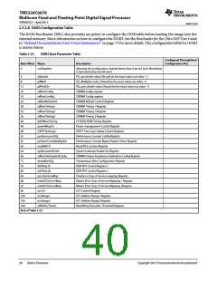
2.5.3.8 DDR3 Configuration Table
The ROM Bootloader (RBL) also provides an option to configure the DDR table before loading the image into the
external memory. More information on how to configure the DDR3, See the Bootloader for the C66x DSP User Guide
in ‘‘Related Documentation from Texas Instruments’’ on page 73 for more details. The configuration table for DDR3
is shown below:
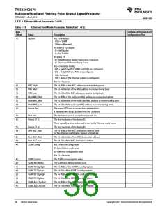
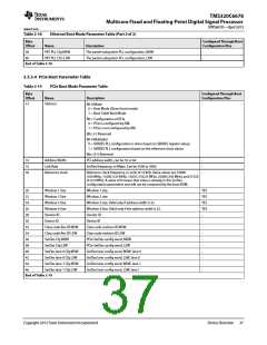
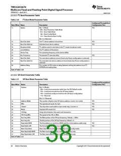
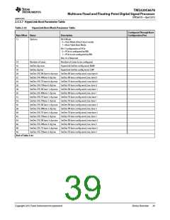
Table 2-23
DDR3 Boot Parameter Table
Configured Through Boot
Configuration Pins
Byte Offset Name
Description
0
configselect
Selecting the configuration register below that to be set. Each filed below
is represented by one bit each.
-
4
pllprediv
PLL pre divider value (Should be the exact value not value -1)
PLL Multiplier value (Should be the exact value not value -1)
PLL post divider value (Should be the exact value not value -1)
SDRAM config register
-
-
-
-
-
-
-
-
-
-
-
-
-
-
-
-
-
-
-
-
-
-
-
-
-
-
-
8
pllMult
12
16
20
24
28
32
36
40
44
48
52
56
60
64
68
72
76
80
84
88
92
96
100
104
108
pllPostDiv
sdRamConfig
sdRamConfig2
sdRamRefreshctl
sdRamTiming1
sdRamTiming2
sdRamTiming3
IpDfrNvmTiming
powerMngCtl
iODFTTestLogic
performcountCfg
performCountMstRegSel
readIdleCtl
SDRAM Config register
SDRAM Refresh Control Register
SDRAM Timing 1 Register
SDRAM Timing 2 Register
SDRAM Timing 3 Register
LP DDR2 NVM Timing Register
Power management Control Register
IODFT Test Logic Global Control Register
Performance Counter Config Register
Performance Counter Master Region Select Register
Read IDLE counter Register
sysVbusmIntEnSet
sdRamOutImpdedCalcfg
tempAlertCfg
ddrPhyCtl1
System Interrupt Enable Set Register
SDRAM Output Impedance Calibration Config Register
Temperature Alert Configuration Register
DDR PHY Control Register 1
ddrPhyCtl2
DDR PHY Control Register 1
proClassSvceMap
mstId2ClsSvce1Map
mstId2ClsSvce2Map
eccCtl
Priority to Class of Service mapping Register
Master ID to Class of Service Mapping 1 Register
Master ID to Class of Service Mapping 2Register
ECC Control Register
eccRange1
ECC Address Range1 Register
eccRange2
ECC Address Range2 Register
rdWrtExcThresh
Read Write Execution Threshold Register
End of Table 2-23
40
Device Overview
Copyright 2013 Texas Instruments Incorporated

 TI [ TEXAS INSTRUMENTS ]