TMS320C6672
Multicore Fixed and Floating-Point Digital Signal Processor
SPRS708C—February 2012
www.ti.com
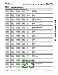
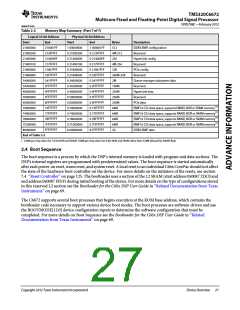
Table 2-2
Memory Map Summary (Part 7 of 7)
Logical 32-bit Address
Physical 36-bit Address
Start
End
Start
End
Bytes
512
Description
21000000
21000200
21400000
21400100
21800000
21808000
34000000
34200000
40000000
50000000
60000000
70000000
74000000
78000000
7C000000
80000000
End of Table 2-2
210001FF
213FFFFF
214000FF
217FFFFF
21807FFF
33FFFFFF
341FFFFF
3FFFFFFF
4FFFFFFF
5FFFFFFF
6FFFFFFF
73FFFFFF
77FFFFFF
7BFFFFFF
7FFFFFFF
FFFFFFFF
1 00000000
0 21000200
0 21400000
0 21400100
0 21800000
0 21808000
0 34000000
0 34200000
0 40000000
0 50000000
0 60000000
0 70000000
0 74000000
0 78000000
0 7C000000
8 00000000
1 000001FF
0 213FFFFF
0 214000FF
0 217FFFFF
0 21807FFF
0 33FFFFFF
0 341FFFFF
0 3FFFFFFF
0 4FFFFFFF
0 5FFFFFFF
0 6FFFFFFF
0 73FFFFFF
0 77FFFFFF
0 7BFFFFFF
0 7FFFFFFF
8 7FFFFFFF
DDR3 EMIF configuration
4M-512
256
Reserved
HyperLink config
4M-256
32K
Reserved
PCIe config
296M-32K
2M
Reserved
Queue manager subsystem data
190M
256M
256M
256M
64M
Reserved
HyperLink data
Reserved
PCIe data
EMIF16 CS2 data space, supports NAND, NOR or SRAM memory (1)
EMIF16 CS3 data space, supports NAND, NOR or SRAM memory(1)
EMIF16 CS4 data space, supports NAND, NOR or SRAM memory(1)
EMIF16 CS5 data space, supports NAND, NOR or SRAM memory(1)
DDR3 EMIF data
64M
64M
64M
2G
1 32MB per chip select for 16-bit NOR and SRAM. 16MB per chip select for 8-bit NOR and SRAM. More than 32MB allowed by NAND flash
2.4 Boot Sequence
The boot sequence is a process by which the DSP's internal memory is loaded with program and data sections. The
DSP's internal registers are programmed with predetermined values. The boot sequence is started automatically
after each power-on reset, warm reset, and system reset. A local reset to an individual C66x CorePac should not affect
the state of the hardware boot controller on the device. For more details on the initiators of the resets, see section
7.4 ‘‘Reset Controller’’ on page 125. The bootloader uses a section of the L2 SRAM (start address 0x0087 2DC0 and
end address 0x0087 FFFF) during initial booting of the device. For more details on the type of configurations stored
in this reserved L2 section see the Bootloader for the C66x DSP User Guide in ‘‘Related Documentation from Texas
Instruments’’ on page 69.
The C6672 supports several boot processes that begins execution at the ROM base address, which contains the
bootloader code necessary to support various device boot modes. The boot processes are software-driven and use
the BOOTMODE[12:0] device configuration inputs to determine the software configuration that must be
completed. For more details on Boot Sequence see the Bootloader for the C66x DSP User Guide in ‘‘Related
Documentation from Texas Instruments’’ on page 69.
Copyright 2012 Texas Instruments Incorporated
Device Overview 27

 TI [ TEXAS INSTRUMENTS ]