TMS320C6672
Multicore Fixed and Floating-Point Digital Signal Processor
SPRS708C—February 2012
www.ti.com
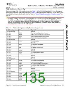
Table 7-14
PLL Controller Registers (Including Reset Controller) (Part 2 of 2)
Hex Address Range
0231 0174 - 0231 0193
0231 0194 - 0231 01FF
End of Table 7-14
Field
Register Name
Reserved
PLLDIV9 - PLLDIV16
-
Reserved
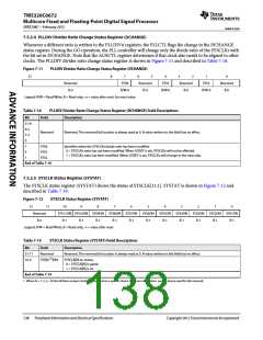
7.5.2.1 PLL Secondary Control Register (SECCTL)
The PLL Secondary Control Register contains extra fields to control the Main PLL and is shown in Figure 7-8 and
described in Table 7-15.
Figure 7-8
PLL Secondary Control Register (SECCTL))
31
24
23
22
19
18
0
Reserved
BYPASS
RW-0
OUTPUT DIVIDE
RW-0001
Reserved
RW-001 0000 0000 0000 0000
R-0000 0000
Legend: R/W = Read/Write; R = Read only; -n = value after reset
Table 7-15
PLL Secondary Control Register (SECCTL) Field Descriptions
Description
Bit
Field
Reserved
31-24
23
Reserved
BYPASS
Main PLL Bypass Enable
0 = Main PLL Bypass disabled
1 = Main PLL Bypass enabled
22-19
OUTPUT DIVIDE
Output Divider ratio bits.
0h = ÷1. Divide frequency by 1.
1h = ÷2. Divide frequency by 2.
2h - Fh = Reserved.
18-0
Reserved
Reserved
End of Table 7-15
136
Peripheral Information and Electrical Specifications
Copyright 2012 Texas Instruments Incorporated

 TI [ TEXAS INSTRUMENTS ]