TMS320C6672
Multicore Fixed and Floating-Point Digital Signal Processor
SPRS708C—February 2012
www.ti.com
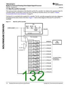
Note—The Main PLL Controller registers can be accessed by any master in the device. The PLLM[5:0] bits
of the multiplier are controlled by the PLLM register inside the PLL controller and PLLM[12:6] bits are
controlled by the chip-level MAINPLLCTL0 register. The Output Divide and Bypass logic of the PLL are
controlled by fields in the SECCTL register in the PLL controller. Only PLLDIV2, PLLDIV5, and PLLDIV8
are programmable on the C6672 device. See the Phase Locked Loop (PLL) Controller for KeyStone Devices
User Guide in ‘‘Related Documentation from Texas Instruments’’ on page 69 for more details on how to
program the PLL controller.
The multiplication and division ratios within the PLL and the post-division for each of the chip-level clocks are
determined by a combination of this PLL and the PLL Controller. The PLL controller also controls reset propagation
through the chip, clock alignment, and test points. The PLL controller monitors the PLL status and provides an
output signal indicating when the PLL is locked.
Main PLL power is supplied externally via the Main PLL power-supply pin (AVDDA1). An external EMI filter
circuit must be added to all PLL supplies. See the Hardware Design Guide for KeyStone Devices in ‘‘Related
Documentation from Texas Instruments’’ on page 69 for detailed recommendations. For the best performance, TI
recommends that all the PLL external components be on a single side of the board without jumpers, switches, or
components other than those shown. For reduced PLL jitter, maximize the spacing between switching signal traces
and the PLL external components (C1, C2, and the EMI Filter).
The minimum SYSCLK rise and fall times should also be observed. For the input clock timing requirements, see
Section 7.5.5 ‘‘Main PLL Controller/SRIO/HyperLink/PCIe Clock Input Electrical Data/Timing’’.
CAUTION—The PLL controller module as described in the see the Phase Locked Loop (PLL) Controller for
KeyStone Devices User Guide in ‘‘Related Documentation from Texas Instruments’’ on page 69 includes a
superset of features, some of which are not supported on the TMS320C6672 device. The following sections
describe the registers that are supported; it should be assumed that any registers not included in these
sections is not supported by the device. Furthermore, only the bits within the registers described here are
supported. Avoid writing to any reserved memory location or changing the value of reserved bits.
7.5.1 Main PLL Controller Device-Specific Information
7.5.1.1 Internal Clocks and Maximum Operating Frequencies
The Main PLL, used to drive the CorePacs, the switch fabric, and a majority of the peripheral clocks (all but the
DDR3 and the network coprocessor (PASS)) requires a PLL controller to manage the various clock divisions, gating,
and synchronization. The Main PLL’s PLL controller has several SYSCLK outputs that are listed below, along with
the clock description. Each SYSCLK has a corresponding divider that divides down the output clock of the PLL. Note
that dividers are not programmable unless explicitly mentioned in the description below.
•
•
SYSCLK1: Full-rate clock for the CorePacs.
SYSCLK2: 1/x-rate clock for CorePac (emulation). Default rate for this will be 1/3. This is programmable from
/1 to /32, where this clock does not violate the max of 350 MHz. The SYSCLK2 can be turned off by software.
•
•
SYSCLK3: 1/2-rate clock used to clock the MSMC, HyperLink, CPU/2 SCR, DDR EMIF and CPU/2 EDMA.
SYSCLK4: 1/3-rate clock for the switch fabrics and fast peripherals. The Debug_SS and ETBs will use this as
well.
•
•
SYSCLK5: 1/y-rate clock for system trace module only. Default rate for this will be 1/5. It is configurable and
the max configurable clock is 210 MHz and min configuration clock is 32 MHz. The SYSCLK5 can be turned
off by software.H
SYSCLK6: 1/64-rate clock. 1/64 rate clock (emif_ptv) used to clock the PVT compensated buffers for DDR3
EMIF.
Copyright 2012 Texas Instruments Incorporated
Peripheral Information and Electrical Specifications 133

 TI [ TEXAS INSTRUMENTS ]